
User manual
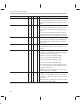
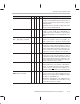
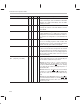
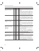
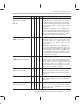
Table Of Contents
- Read This First
- Contents
- Figures
- Tables
- Examples
- Cautions
- Introduction
- Architectural Overview
- Central Processing Unit
- Memory and I/O Spaces
- Program Control
- Addressing Modes
- Assembly Language Instructions
- Instruction Set Summary
- How To Use the Instruction Descriptions
- Instruction Descriptions
- ABS
- ABS
- ADD
- ADD
- ADD
- ADD
- ADDC
- ADDC
- ADDS
- ADDS
- ADDT
- ADDT
- ADRK
- AND
- AND
- AND
- APAC
- APAC
- B
- BACC
- BANZ
- BANZ
- BCND
- BCND
- BIT
- BIT
- BITT
- BITT
- BLDD
- BLDD
- BLDD
- BLDD
- BLDD
- BLPD
- BLPD
- BLPD
- BLPD
- CALA
- CALL
- CC
- CC
- CLRC
- CLRC
- CMPL
- CMPR
- DMOV
- DMOV
- IDLE
- IN
- IN
- INTR
- LACC
- LACC
- LACC
- LACL
- LACL
- LACL
- LACT
- LACT
- LAR
- LAR
- LAR
- LDP
- LDP
- LPH
- LPH
- LST
- LST
- LST
- LST
- LT
- LT
- LTA
- LTA
- LTD
- LTD
- LTD
- LTP
- LTP
- LTS
- LTS
- MAC
- MAC
- MAC
- MAC
- MACD
- MACD
- MACD
- MACD
- MACD
- MAR
- MAR
- MPY
- MPY
- MPY
- MPYA
- MPYA
- MPYS
- MPYS
- MPYU
- MPYU
- NEG
- NEG
- NMI
- NOP
- NORM
- NORM
- NORM
- OR
- OR
- OR
- OUT
- OUT
- PAC
- POP
- POP
- POPD
- POPD
- PSHD
- PSHD
- PUSH
- RET
- RETC
- ROL
- ROR
- RPT
- RPT
- SACH
- SACH
- SACL
- SACL
- SAR
- SAR
- SBRK
- SETC
- SETC
- SFL
- SFR
- SFR
- SPAC
- SPH
- SPH
- SPL
- SPL
- SPLK
- SPLK
- SPM
- SQRA
- SQRA
- SQRS
- SQRS
- SST
- SST
- SUB
- SUB
- SUB
- SUB
- SUBB
- SUBB
- SUBC
- SUBC
- SUBS
- SUBS
- SUBT
- SUBT
- TBLR
- TBLR
- TBLR
- TBLW
- TBLW
- TBLW
- TRAP
- XOR
- XOR
- XOR
- ZALR
- ZALR
- On-Chip Peripherals
- Synchronous Serial Port
- Asynchronous Serial Port
- TMS320C209
- Register Summary
- TMS320C1x/C2x/C2xx/C5x Instruction Set Comparison
- Program Examples
- Submitting ROM Codes to TI
- Design Considerations for Using XDS510 Emulator
- E.1 Designing Your Target System’s Emulator Connector (14-Pin Header)
- E.2 Bus Protocol
- E.3 Emulator Cable Pod
- E.4 Emulator Cable Pod Signal Timing
- E.5 Emulation Timing Calculations
- E.6 Connections Between the Emulator and the Target System
- E.7 Physical Dimensions for the 14-Pin Emulator Connector
- E.8 Emulation Design Considerations
- Glossary
- Index

Instruction Set Comparison Table
B-17
TMS320C1x/C2x/C2xx/C5x Instruction Set Comparison
Syntax
Description5x2xx2x1x
CNFP
√ √ √
Configure Block as Program Memory
Configure on-chip RAM block B0 as program memory.
Block B0 is mapped into program-memory locations
65280h–65535h.
TMS320C5x devices: Block B0 is mapped into data-
memory locations 65024h–65535h.
CONF
2-bit constant
√
Configure Block as Program Memory
Configure on-chip RAM block B0/B1/B2/B3 as
program memory. For information on the memory
mapping of B0/B1/B2/B3, see the
TMS320C2x User’s
Guide
.
CPL [
#
lk,
]
dma
CPL [
#
lk,
] {
ind
} [
, next ARP
]
√
√
Compare DBMR or Immediate With Data Value
Compare two quantities: If the two quantities are
equal, set the TC bit to 1; otherwise, clear the TC bit.
CRGT
√
Test for ACC > ACCB
Compare the contents of the ACC with the contents of
the ACCB, then load the larger signed value into both
registers and modify the carry bit according to the com-
parison result. If the contents of ACC are greater than
or equal to the contents of ACCB, set the carry bit to 1.
CRLT
√
Test for ACC < ACCB
Compare the contents of the ACC with the contents of
the ACCB, then load the smaller signed value into both
registers and modify the carry bit according to the com-
parison result. If the contents of ACC are less than the
contents of ACCB, clear the carry bit.
DINT
√ √ √ √
Disable Interrupts
Disable all interrupts; set the INTM to 1. Maskable in-
terrupts are disabled immediately after the DINT in-
struction executes. DINT does not disable the un-
maskable interrupt RS
; DINT does not affect the IMR.
DMOV
dma
DMOV {
ind
} [
, next ARP
]
√
√
√
√
√
√
√
√
Data Move in Data Memory
Copy the contents of the addressed data-memory lo-
cation into the next higher address. DMOV moves data
only within on-chip RAM blocks.
TMS320C2x, TMS320C2xx, and TMS320C5x de-
vices: The on-chip RAM blocks are B0 (when config-
ured as data memory), B1, and B2.