
User manual
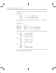
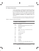
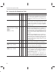
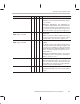
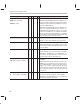
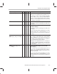
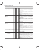
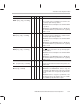
Table Of Contents
- Read This First
- Contents
- Figures
- Tables
- Examples
- Cautions
- Introduction
- Architectural Overview
- Central Processing Unit
- Memory and I/O Spaces
- Program Control
- Addressing Modes
- Assembly Language Instructions
- Instruction Set Summary
- How To Use the Instruction Descriptions
- Instruction Descriptions
- ABS
- ABS
- ADD
- ADD
- ADD
- ADD
- ADDC
- ADDC
- ADDS
- ADDS
- ADDT
- ADDT
- ADRK
- AND
- AND
- AND
- APAC
- APAC
- B
- BACC
- BANZ
- BANZ
- BCND
- BCND
- BIT
- BIT
- BITT
- BITT
- BLDD
- BLDD
- BLDD
- BLDD
- BLDD
- BLPD
- BLPD
- BLPD
- BLPD
- CALA
- CALL
- CC
- CC
- CLRC
- CLRC
- CMPL
- CMPR
- DMOV
- DMOV
- IDLE
- IN
- IN
- INTR
- LACC
- LACC
- LACC
- LACL
- LACL
- LACL
- LACT
- LACT
- LAR
- LAR
- LAR
- LDP
- LDP
- LPH
- LPH
- LST
- LST
- LST
- LST
- LT
- LT
- LTA
- LTA
- LTD
- LTD
- LTD
- LTP
- LTP
- LTS
- LTS
- MAC
- MAC
- MAC
- MAC
- MACD
- MACD
- MACD
- MACD
- MACD
- MAR
- MAR
- MPY
- MPY
- MPY
- MPYA
- MPYA
- MPYS
- MPYS
- MPYU
- MPYU
- NEG
- NEG
- NMI
- NOP
- NORM
- NORM
- NORM
- OR
- OR
- OR
- OUT
- OUT
- PAC
- POP
- POP
- POPD
- POPD
- PSHD
- PSHD
- PUSH
- RET
- RETC
- ROL
- ROR
- RPT
- RPT
- SACH
- SACH
- SACL
- SACL
- SAR
- SAR
- SBRK
- SETC
- SETC
- SFL
- SFR
- SFR
- SPAC
- SPH
- SPH
- SPL
- SPL
- SPLK
- SPLK
- SPM
- SQRA
- SQRA
- SQRS
- SQRS
- SST
- SST
- SUB
- SUB
- SUB
- SUB
- SUBB
- SUBB
- SUBC
- SUBC
- SUBS
- SUBS
- SUBT
- SUBT
- TBLR
- TBLR
- TBLR
- TBLW
- TBLW
- TBLW
- TRAP
- XOR
- XOR
- XOR
- ZALR
- ZALR
- On-Chip Peripherals
- Synchronous Serial Port
- Asynchronous Serial Port
- TMS320C209
- Register Summary
- TMS320C1x/C2x/C2xx/C5x Instruction Set Comparison
- Program Examples
- Submitting ROM Codes to TI
- Design Considerations for Using XDS510 Emulator
- E.1 Designing Your Target System’s Emulator Connector (14-Pin Header)
- E.2 Bus Protocol
- E.3 Emulator Cable Pod
- E.4 Emulator Cable Pod Signal Timing
- E.5 Emulation Timing Calculations
- E.6 Connections Between the Emulator and the Target System
- E.7 Physical Dimensions for the 14-Pin Emulator Connector
- E.8 Emulation Design Considerations
- Glossary
- Index

Instruction Set Comparison Table
B-8
Syntax
Description5x2xx2x1x
AND
dma
AND {
ind
}
[
, next ARP
]
AND #
lk
[
, shift
]
√
√
√
√
√
√
√
√
√
√
AND With Accumulator
TMS320C1x and TMS320C2x devices: AND the con-
tents of the addressed data-memory location with the
16 LSBs of the accumulator. The 16 MSBs of the accu-
mulator are ANDed with 0s.
TMS320C2xx and TMS320C5x devices: AND the con-
tents of the addressed data-memory location or a
16-bit immediate value with the contents of the accu-
mulator. The 16 MSBs of the accumulator are ANDed
with 0s. If a shift is specified, left shift the constant be-
fore the AND. Low-order bits below and high-order bits
above the shifted value are treated as 0s.
ANDB
√
AND ACCB to Accumulator
AND the contents of the ACCB to the accumulator.
ANDK #
lk
[
, shift
]
√ √ √
AND Immediate With Accumulator With Shift
AND a 16-bit immediate value with the contents of the
accumulator; if a shift is specified, left shift the constant
before the AND.
APAC
√ √ √ √
Add P Register to Accumulator
Add the contents of the P register to the accumulator.
TMS320C2x, TMS320C2xx, and TMS320C5x de-
vices: Before the add, left shift the contents of the P
register as defined by the PM status bits.
APL [#
lk
]
,dma
APL [#
lk,
]
{
ind
} [
, next ARP
]
√
√
AND Data-Memory Value With DBMR or Long
Constant
AND the data-memory value with the contents of the
DBMR or a long constant. If a long constant is speci-
fied, it is ANDed with the contents of the data-memory
location. The result is written back into the data-
memory location previously holding the first operand.
If the result is 0, the TC bit is set to 1; otherwise, the TC
bit is cleared.
B
pma
B
pma
[
,
{
ind
} [
, next ARP
]]
√
√ √
Branch Unconditionally
Branch to the specified program-memory address.
TMS320C2x and TMS320C2xx devices: Modify the
current AR and ARP as specified.