
User manual
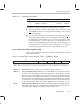
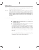
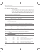
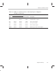
Table Of Contents
- Read This First
- Contents
- Figures
- Tables
- Examples
- Cautions
- Introduction
- Architectural Overview
- Central Processing Unit
- Memory and I/O Spaces
- Program Control
- Addressing Modes
- Assembly Language Instructions
- Instruction Set Summary
- How To Use the Instruction Descriptions
- Instruction Descriptions
- ABS
- ABS
- ADD
- ADD
- ADD
- ADD
- ADDC
- ADDC
- ADDS
- ADDS
- ADDT
- ADDT
- ADRK
- AND
- AND
- AND
- APAC
- APAC
- B
- BACC
- BANZ
- BANZ
- BCND
- BCND
- BIT
- BIT
- BITT
- BITT
- BLDD
- BLDD
- BLDD
- BLDD
- BLDD
- BLPD
- BLPD
- BLPD
- BLPD
- CALA
- CALL
- CC
- CC
- CLRC
- CLRC
- CMPL
- CMPR
- DMOV
- DMOV
- IDLE
- IN
- IN
- INTR
- LACC
- LACC
- LACC
- LACL
- LACL
- LACL
- LACT
- LACT
- LAR
- LAR
- LAR
- LDP
- LDP
- LPH
- LPH
- LST
- LST
- LST
- LST
- LT
- LT
- LTA
- LTA
- LTD
- LTD
- LTD
- LTP
- LTP
- LTS
- LTS
- MAC
- MAC
- MAC
- MAC
- MACD
- MACD
- MACD
- MACD
- MACD
- MAR
- MAR
- MPY
- MPY
- MPY
- MPYA
- MPYA
- MPYS
- MPYS
- MPYU
- MPYU
- NEG
- NEG
- NMI
- NOP
- NORM
- NORM
- NORM
- OR
- OR
- OR
- OUT
- OUT
- PAC
- POP
- POP
- POPD
- POPD
- PSHD
- PSHD
- PUSH
- RET
- RETC
- ROL
- ROR
- RPT
- RPT
- SACH
- SACH
- SACL
- SACL
- SAR
- SAR
- SBRK
- SETC
- SETC
- SFL
- SFR
- SFR
- SPAC
- SPH
- SPH
- SPL
- SPL
- SPLK
- SPLK
- SPM
- SQRA
- SQRA
- SQRS
- SQRS
- SST
- SST
- SUB
- SUB
- SUB
- SUB
- SUBB
- SUBB
- SUBC
- SUBC
- SUBS
- SUBS
- SUBT
- SUBT
- TBLR
- TBLR
- TBLR
- TBLW
- TBLW
- TBLW
- TRAP
- XOR
- XOR
- XOR
- ZALR
- ZALR
- On-Chip Peripherals
- Synchronous Serial Port
- Asynchronous Serial Port
- TMS320C209
- Register Summary
- TMS320C1x/C2x/C2xx/C5x Instruction Set Comparison
- Program Examples
- Submitting ROM Codes to TI
- Design Considerations for Using XDS510 Emulator
- E.1 Designing Your Target System’s Emulator Connector (14-Pin Header)
- E.2 Bus Protocol
- E.3 Emulator Cable Pod
- E.4 Emulator Cable Pod Signal Timing
- E.5 Emulation Timing Calculations
- E.6 Connections Between the Emulator and the Target System
- E.7 Physical Dimensions for the 14-Pin Emulator Connector
- E.8 Emulation Design Considerations
- Glossary
- Index
Register Descriptions
A-5
Register Summary
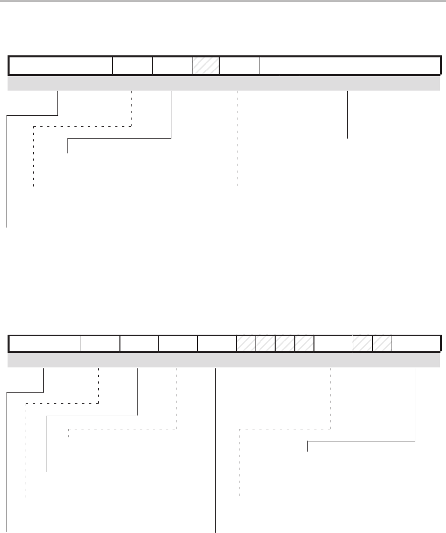
Status Register ST0
15 14 13 12 11 10 9 8 7 6 5 4 3 2 1 0
X X X 0 X 1
†
1 X X X X X X X X X
ARP OV OVM INTM DP
All unmasked interrupts enabled
All unmasked interrupts disabled
0
1
Auxiliary register pointer
Selects the current page
(0, 1, 2, ..., 511) in
data memory
Data page pointer
R/W R/W R/W
Selects the current auxiliary register
(0, 1, 2, 3, 4, 5, 6, or 7)
R/W
Accumulator results overflow normally.
Overflow mode selected
0
1
Flag is reset
Overflow detected in accumulator
0
1
R/W
Interrupt mode
Overflow mode
Overflow flag
†
This reserved bit is always read as 1. Writes have no effect.
Status Register ST1
151413 12 11 10 9 8765 4 32 1 0
XXX 0 X 1 11
†
1
†
1
†
1
†
11
†
1
†
00
ARB CNF TC SXM C XF PM
Auxiliary register pointer buffer
Product shift mode
R/W R/W R/W
Holds previous ARP value
R/W
Holds results of various software tests
DARAM B0 mapped to data memory
DARAM B0 mapped to program memory
0
1
R/WR/W
Test/control flag
Sign extension suppressed
Sign extension mode selected
0
1
R/W
Carry not generated/borrow generated
Carry generated/borrow not generated
0
1
XF pin low
XF pin high
0
1
No shift
Left shift of 1
Left shift of 4
Right shift of 6, sign extended
0
1
0
1
0
0
1
1
Carry bit
XF pin status
Sign-extension mode
DARAM B0 configuration
†
These reserved bits are always read as 1s. Writes have no effect.