
User manual
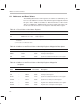
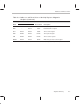
Table Of Contents
- Read This First
- Contents
- Figures
- Tables
- Examples
- Cautions
- Introduction
- Architectural Overview
- Central Processing Unit
- Memory and I/O Spaces
- Program Control
- Addressing Modes
- Assembly Language Instructions
- Instruction Set Summary
- How To Use the Instruction Descriptions
- Instruction Descriptions
- ABS
- ABS
- ADD
- ADD
- ADD
- ADD
- ADDC
- ADDC
- ADDS
- ADDS
- ADDT
- ADDT
- ADRK
- AND
- AND
- AND
- APAC
- APAC
- B
- BACC
- BANZ
- BANZ
- BCND
- BCND
- BIT
- BIT
- BITT
- BITT
- BLDD
- BLDD
- BLDD
- BLDD
- BLDD
- BLPD
- BLPD
- BLPD
- BLPD
- CALA
- CALL
- CC
- CC
- CLRC
- CLRC
- CMPL
- CMPR
- DMOV
- DMOV
- IDLE
- IN
- IN
- INTR
- LACC
- LACC
- LACC
- LACL
- LACL
- LACL
- LACT
- LACT
- LAR
- LAR
- LAR
- LDP
- LDP
- LPH
- LPH
- LST
- LST
- LST
- LST
- LT
- LT
- LTA
- LTA
- LTD
- LTD
- LTD
- LTP
- LTP
- LTS
- LTS
- MAC
- MAC
- MAC
- MAC
- MACD
- MACD
- MACD
- MACD
- MACD
- MAR
- MAR
- MPY
- MPY
- MPY
- MPYA
- MPYA
- MPYS
- MPYS
- MPYU
- MPYU
- NEG
- NEG
- NMI
- NOP
- NORM
- NORM
- NORM
- OR
- OR
- OR
- OUT
- OUT
- PAC
- POP
- POP
- POPD
- POPD
- PSHD
- PSHD
- PUSH
- RET
- RETC
- ROL
- ROR
- RPT
- RPT
- SACH
- SACH
- SACL
- SACL
- SAR
- SAR
- SBRK
- SETC
- SETC
- SFL
- SFR
- SFR
- SPAC
- SPH
- SPH
- SPL
- SPL
- SPLK
- SPLK
- SPM
- SQRA
- SQRA
- SQRS
- SQRS
- SST
- SST
- SUB
- SUB
- SUB
- SUB
- SUBB
- SUBB
- SUBC
- SUBC
- SUBS
- SUBS
- SUBT
- SUBT
- TBLR
- TBLR
- TBLR
- TBLW
- TBLW
- TBLW
- TRAP
- XOR
- XOR
- XOR
- ZALR
- ZALR
- On-Chip Peripherals
- Synchronous Serial Port
- Asynchronous Serial Port
- TMS320C209
- Register Summary
- TMS320C1x/C2x/C2xx/C5x Instruction Set Comparison
- Program Examples
- Submitting ROM Codes to TI
- Design Considerations for Using XDS510 Emulator
- E.1 Designing Your Target System’s Emulator Connector (14-Pin Header)
- E.2 Bus Protocol
- E.3 Emulator Cable Pod
- E.4 Emulator Cable Pod Signal Timing
- E.5 Emulation Timing Calculations
- E.6 Connections Between the Emulator and the Target System
- E.7 Physical Dimensions for the 14-Pin Emulator Connector
- E.8 Emulation Design Considerations
- Glossary
- Index

Addresses and Reset Values
A-2
A.1 Addresses and Reset Values
The following tables list the ’C2xx registers, the addresses at which they can
be accessed, and their reset values. Note that the registers mapped to internal
I/O space on the ’C209 are at addresses different from those of other ’C2xx
devices. In addition, the ’C209 wait-state generator control register has a dif-
ferent reset value because there are only four control bits in the register.
Table A–1. Reset Values of the Status Registers
Name Reset Value (Binary) Description
ST0 XXX0 X11X XXXX XXXX Status register 0
ST1 XXX0 X111 1111 1100 Status register 1
Notes: 1) No addresses are given for ST0 and ST1 because they can be accessed only by the CLRC, SETC, LST, and SST
instructions.
2) X: Reset does not affect these bits.
Table A–2. Addresses and Reset Values of On-Chip Registers Mapped to Data Space
Name Data-Memory Address Reset Value Description
IMR 0004h 0000h Interrupt mask register
GREG 0005h 0000h Interrupt control register
IFR 0006h 0000h Synchronous data transmit and receive register
Note: An x in an address represents four bits that are either not affected by reset or dependent on pin levels at reset.
Table A–3. Addresses and Reset Values of On-Chip Registers Mapped to
I/O Space
I/O Address
Name ’C209 Other ’C2xx Reset Value Description
CLK
– FFE8h 0000h CLKOUT1-pin control (CLK) register
ICR – FFECh 0000h Interrupt control register
SDTR – FFF0h xxxxh Synchronous data transmit and receive register
SSPCR – FFF1h 0030h Synchronous serial port control register
ADTR – FFF4h xxxxh Asynchronous data transmit and receive register
ASPCR – FFF5h 0000h Asynchronous serial port control register
Note: An x in an address represents four bits that are either not affected by reset or dependent on pin levels at reset.