
User manual
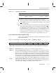
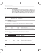
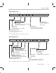
Table Of Contents
- Read This First
- Contents
- Figures
- Tables
- Examples
- Cautions
- Introduction
- Architectural Overview
- Central Processing Unit
- Memory and I/O Spaces
- Program Control
- Addressing Modes
- Assembly Language Instructions
- Instruction Set Summary
- How To Use the Instruction Descriptions
- Instruction Descriptions
- ABS
- ABS
- ADD
- ADD
- ADD
- ADD
- ADDC
- ADDC
- ADDS
- ADDS
- ADDT
- ADDT
- ADRK
- AND
- AND
- AND
- APAC
- APAC
- B
- BACC
- BANZ
- BANZ
- BCND
- BCND
- BIT
- BIT
- BITT
- BITT
- BLDD
- BLDD
- BLDD
- BLDD
- BLDD
- BLPD
- BLPD
- BLPD
- BLPD
- CALA
- CALL
- CC
- CC
- CLRC
- CLRC
- CMPL
- CMPR
- DMOV
- DMOV
- IDLE
- IN
- IN
- INTR
- LACC
- LACC
- LACC
- LACL
- LACL
- LACL
- LACT
- LACT
- LAR
- LAR
- LAR
- LDP
- LDP
- LPH
- LPH
- LST
- LST
- LST
- LST
- LT
- LT
- LTA
- LTA
- LTD
- LTD
- LTD
- LTP
- LTP
- LTS
- LTS
- MAC
- MAC
- MAC
- MAC
- MACD
- MACD
- MACD
- MACD
- MACD
- MAR
- MAR
- MPY
- MPY
- MPY
- MPYA
- MPYA
- MPYS
- MPYS
- MPYU
- MPYU
- NEG
- NEG
- NMI
- NOP
- NORM
- NORM
- NORM
- OR
- OR
- OR
- OUT
- OUT
- PAC
- POP
- POP
- POPD
- POPD
- PSHD
- PSHD
- PUSH
- RET
- RETC
- ROL
- ROR
- RPT
- RPT
- SACH
- SACH
- SACL
- SACL
- SAR
- SAR
- SBRK
- SETC
- SETC
- SFL
- SFR
- SFR
- SPAC
- SPH
- SPH
- SPL
- SPL
- SPLK
- SPLK
- SPM
- SQRA
- SQRA
- SQRS
- SQRS
- SST
- SST
- SUB
- SUB
- SUB
- SUB
- SUBB
- SUBB
- SUBC
- SUBC
- SUBS
- SUBS
- SUBT
- SUBT
- TBLR
- TBLR
- TBLR
- TBLW
- TBLW
- TBLW
- TRAP
- XOR
- XOR
- XOR
- ZALR
- ZALR
- On-Chip Peripherals
- Synchronous Serial Port
- Asynchronous Serial Port
- TMS320C209
- Register Summary
- TMS320C1x/C2x/C2xx/C5x Instruction Set Comparison
- Program Examples
- Submitting ROM Codes to TI
- Design Considerations for Using XDS510 Emulator
- E.1 Designing Your Target System’s Emulator Connector (14-Pin Header)
- E.2 Bus Protocol
- E.3 Emulator Cable Pod
- E.4 Emulator Cable Pod Signal Timing
- E.5 Emulation Timing Calculations
- E.6 Connections Between the Emulator and the Target System
- E.7 Physical Dimensions for the 14-Pin Emulator Connector
- E.8 Emulation Design Considerations
- Glossary
- Index

’C209 On-Chip Peripherals
11-17
TMS320C209
Figure 11–5.’C209 Wait-State Generator Control Register (WSGR) — I/O Address FFFFh
15–4 3 2 1 0
Reserved AVIS ISWS DSWS PSWS
0 W–1 W–1 W–1 W–1
Note: 0 = Always read as zeros; W = Write access; value following dash (–) is value after reset.
Bits 15–4 Reserved. Bits 15–4 are reserved and are always read as 0s.
Bit 3 AVIS — Address visibility mode. AVIS = 1 enables the address visibility mode of
the device. In this mode, the device provides a method of tracing internal code opera-
tion: it passes the internal program address to the address bus when this bus is not
used for an external access. At reset, AVIS is set to 1. For production systems, the
AVIS bit should be cleared to 0 to reduce power and noise. (AVIS does not generate
a wait state.)
Bit 2 ISWS — I/O-space wait-state bit. When ISWS = 1, one wait state will be applied to
all reads from off-chip I/O space. When ISWS = 0, no wait states are generated for
off-chip I/O space. At reset, this bit is set to 1.
Bit 1 DSWS — Data-space wait-state bit. When DSWS = 1, one wait state will be applied
to all reads from off-chip data space. When DSWS = 0, no wait states are generated
for off-chip data space. At reset, this bit is set to 1.
Bit 0 PSWS — Program-space wait-state bit. When PSWS = 1, one wait state will be ap-
plied to all reads from off-chip program space. When PSWS = 0, no wait states are
generated for off-chip program space. At reset, this bit is set to 1.