
User manual
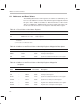
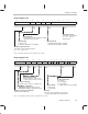
Table Of Contents
- Read This First
- Contents
- Figures
- Tables
- Examples
- Cautions
- Introduction
- Architectural Overview
- Central Processing Unit
- Memory and I/O Spaces
- Program Control
- Addressing Modes
- Assembly Language Instructions
- Instruction Set Summary
- How To Use the Instruction Descriptions
- Instruction Descriptions
- ABS
- ABS
- ADD
- ADD
- ADD
- ADD
- ADDC
- ADDC
- ADDS
- ADDS
- ADDT
- ADDT
- ADRK
- AND
- AND
- AND
- APAC
- APAC
- B
- BACC
- BANZ
- BANZ
- BCND
- BCND
- BIT
- BIT
- BITT
- BITT
- BLDD
- BLDD
- BLDD
- BLDD
- BLDD
- BLPD
- BLPD
- BLPD
- BLPD
- CALA
- CALL
- CC
- CC
- CLRC
- CLRC
- CMPL
- CMPR
- DMOV
- DMOV
- IDLE
- IN
- IN
- INTR
- LACC
- LACC
- LACC
- LACL
- LACL
- LACL
- LACT
- LACT
- LAR
- LAR
- LAR
- LDP
- LDP
- LPH
- LPH
- LST
- LST
- LST
- LST
- LT
- LT
- LTA
- LTA
- LTD
- LTD
- LTD
- LTP
- LTP
- LTS
- LTS
- MAC
- MAC
- MAC
- MAC
- MACD
- MACD
- MACD
- MACD
- MACD
- MAR
- MAR
- MPY
- MPY
- MPY
- MPYA
- MPYA
- MPYS
- MPYS
- MPYU
- MPYU
- NEG
- NEG
- NMI
- NOP
- NORM
- NORM
- NORM
- OR
- OR
- OR
- OUT
- OUT
- PAC
- POP
- POP
- POPD
- POPD
- PSHD
- PSHD
- PUSH
- RET
- RETC
- ROL
- ROR
- RPT
- RPT
- SACH
- SACH
- SACL
- SACL
- SAR
- SAR
- SBRK
- SETC
- SETC
- SFL
- SFR
- SFR
- SPAC
- SPH
- SPH
- SPL
- SPL
- SPLK
- SPLK
- SPM
- SQRA
- SQRA
- SQRS
- SQRS
- SST
- SST
- SUB
- SUB
- SUB
- SUB
- SUBB
- SUBB
- SUBC
- SUBC
- SUBS
- SUBS
- SUBT
- SUBT
- TBLR
- TBLR
- TBLR
- TBLW
- TBLW
- TBLW
- TRAP
- XOR
- XOR
- XOR
- ZALR
- ZALR
- On-Chip Peripherals
- Synchronous Serial Port
- Asynchronous Serial Port
- TMS320C209
- Register Summary
- TMS320C1x/C2x/C2xx/C5x Instruction Set Comparison
- Program Examples
- Submitting ROM Codes to TI
- Design Considerations for Using XDS510 Emulator
- E.1 Designing Your Target System’s Emulator Connector (14-Pin Header)
- E.2 Bus Protocol
- E.3 Emulator Cable Pod
- E.4 Emulator Cable Pod Signal Timing
- E.5 Emulation Timing Calculations
- E.6 Connections Between the Emulator and the Target System
- E.7 Physical Dimensions for the 14-Pin Emulator Connector
- E.8 Emulation Design Considerations
- Glossary
- Index

’C209 On-Chip Peripherals
11-14
11.4 ’C209 On-Chip Peripherals
The ’C209 has these on-chip peripherals:
Clock generator. The clock generator is fundamentally the same on all
’C2xx devices, including the ’C209. However, the ’C209 is limited to the
two clock modes described in subsection 11.4.1.
Timer. The timer is also fundamentally the same. The difference here is
that the timer control register (TCR) on the ’C209 does not offer bits for
configuring timer emulation modes. Subsection 11.4.2 describes the
’C209 TCR.
Wait-state generator. The wait-state generators of the ’C2xx devices op-
erate similarly; however, the ’C209 wait-state generator is different from
that of other ’C2xx devices in these ways:
It offers zero or one wait states (not zero to seven).
It cannot produce separate wait states for the lower (0000h–7FFFh)
and upper (8000h–FFFFh) halves of program space.
It provides a bit for enabling or disabling address visibility mode. In this
mode (not available on other ’C2xx devices), the ’C209 passes the in-
ternal program address to the external address bus when this bus is
not used for an external access.
The ’C209 generator is programmable by way of the ’C209 wait-state gen-
erator control register (WSGR) and is described subsection 11.4.3.
11.4.1 ’C209 Clock Generator Options
The ’C209 includes two clock modes: divide-by-2 (÷2) and multiply-by-2 (×2).
The
÷2 mode operates the CPU at half the input clock rate. The ×2 option
doubles the input clock and phase-locks the output clock with the input clock.
To enable the
÷2 mode, tie the CLKMOD pin low. To enable the ×2 mode, tie
CLKMOD high. For each clock mode, Table 11–5 shows the generated CPU
clock rate and shows the state of CLKMOD, the internal oscillator, and the in-
ternal phase lock loop (PLL).
Notes:
Change CLKMOD only while the reset signal (RS or RS) is active.
The PLL requires approximately 2200 cycles to lock the output clock sig-
nal to the input clock signal. When setting the ×2 mode, keep the reset
(RS
or RS) signal active until at least three cycles after the PLL has stabi-
lized.