
User manual
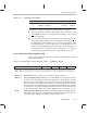
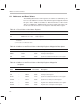
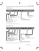
Table Of Contents
- Read This First
- Contents
- Figures
- Tables
- Examples
- Cautions
- Introduction
- Architectural Overview
- Central Processing Unit
- Memory and I/O Spaces
- Program Control
- Addressing Modes
- Assembly Language Instructions
- Instruction Set Summary
- How To Use the Instruction Descriptions
- Instruction Descriptions
- ABS
- ABS
- ADD
- ADD
- ADD
- ADD
- ADDC
- ADDC
- ADDS
- ADDS
- ADDT
- ADDT
- ADRK
- AND
- AND
- AND
- APAC
- APAC
- B
- BACC
- BANZ
- BANZ
- BCND
- BCND
- BIT
- BIT
- BITT
- BITT
- BLDD
- BLDD
- BLDD
- BLDD
- BLDD
- BLPD
- BLPD
- BLPD
- BLPD
- CALA
- CALL
- CC
- CC
- CLRC
- CLRC
- CMPL
- CMPR
- DMOV
- DMOV
- IDLE
- IN
- IN
- INTR
- LACC
- LACC
- LACC
- LACL
- LACL
- LACL
- LACT
- LACT
- LAR
- LAR
- LAR
- LDP
- LDP
- LPH
- LPH
- LST
- LST
- LST
- LST
- LT
- LT
- LTA
- LTA
- LTD
- LTD
- LTD
- LTP
- LTP
- LTS
- LTS
- MAC
- MAC
- MAC
- MAC
- MACD
- MACD
- MACD
- MACD
- MACD
- MAR
- MAR
- MPY
- MPY
- MPY
- MPYA
- MPYA
- MPYS
- MPYS
- MPYU
- MPYU
- NEG
- NEG
- NMI
- NOP
- NORM
- NORM
- NORM
- OR
- OR
- OR
- OUT
- OUT
- PAC
- POP
- POP
- POPD
- POPD
- PSHD
- PSHD
- PUSH
- RET
- RETC
- ROL
- ROR
- RPT
- RPT
- SACH
- SACH
- SACL
- SACL
- SAR
- SAR
- SBRK
- SETC
- SETC
- SFL
- SFR
- SFR
- SPAC
- SPH
- SPH
- SPL
- SPL
- SPLK
- SPLK
- SPM
- SQRA
- SQRA
- SQRS
- SQRS
- SST
- SST
- SUB
- SUB
- SUB
- SUB
- SUBB
- SUBB
- SUBC
- SUBC
- SUBS
- SUBS
- SUBT
- SUBT
- TBLR
- TBLR
- TBLR
- TBLW
- TBLW
- TBLW
- TRAP
- XOR
- XOR
- XOR
- ZALR
- ZALR
- On-Chip Peripherals
- Synchronous Serial Port
- Asynchronous Serial Port
- TMS320C209
- Register Summary
- TMS320C1x/C2x/C2xx/C5x Instruction Set Comparison
- Program Examples
- Submitting ROM Codes to TI
- Design Considerations for Using XDS510 Emulator
- E.1 Designing Your Target System’s Emulator Connector (14-Pin Header)
- E.2 Bus Protocol
- E.3 Emulator Cable Pod
- E.4 Emulator Cable Pod Signal Timing
- E.5 Emulation Timing Calculations
- E.6 Connections Between the Emulator and the Target System
- E.7 Physical Dimensions for the 14-Pin Emulator Connector
- E.8 Emulation Design Considerations
- Glossary
- Index

’C209 Interrupts
11-13
TMS320C209
Figure 11–3.’C209 Interrupt Mask Register (IMR) — Data-Memory Address 0004h
15 4 3 2 1 0
Reserved TINT INT3 INT2 INT1
0 R/W–0 R/W–0 R/W–0 R/W–0
Note: Note: 0 = Always read as zeros; R = Read access; W = Write access; value following dash (–) is value after reset.
Bits 15–4 Reserved. Bits 15–4 are reserved and are always read as 0s.
Bit 3 TINT — Timer interrupt mask. Mask or unmask the internal timer interrupt, TINT, with
this bit.
TINT = 0 TINT is unmasked.
TINT = 1 TINT is masked.
Bit 2 INT3 — Interrupt 3 mask. Unmask external interrupt INT3
by writing a 1 to this bit.
INT3 = 0 INT3
is unmasked.
INT3 = 1 INT3
is masked.
Bit 1 INT2 — Interrupt 2 mask. Unmask external interrupt INT2
by writing a 1 to this bit.
INT2 = 0 INT2
is unmasked.
INT2 = 1 INT2
is masked.
Bit 0 INT1 — Interrupt 1 mask. Unmask external interrupt INT1
by writing a 1 to this bit.
INT1 = 0 INT1
is unmasked.
INT1 = 1 INT1
is masked.
11.3.2 IACK Pin
On the ’C209, the interrupt acknowledge signal is available at the external
IACK
pin. The CPU generates this signal while it fetches the first word of any
of the interrupt vectors, whether the interrupt was requested by hardware or
by software. IACK
is not affected by wait states; IACK goes low only on the first
cycle of the read when wait states are used. At reset, the interrupt acknowl-
edge signal is generated in the same manner as for a maskable interrupt.
Your external hardware can use the IACK
signal to determine when the pro-
cessor acknowledges an interrupt. Additionally, when IACK
goes low, the
hardware can sample the address pins (A15–A0) to determine which interrupt
the processor is acknowledging. Since the interrupt vectors are spaced apart
by two words, address pins A1–A4 can be decoded at the falling edge of IACK
to identify the interrupt being acknowledged.