
User manual
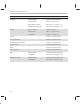
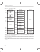

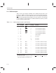
Table Of Contents
- Read This First
- Contents
- Figures
- Tables
- Examples
- Cautions
- Introduction
- Architectural Overview
- Central Processing Unit
- Memory and I/O Spaces
- Program Control
- Addressing Modes
- Assembly Language Instructions
- Instruction Set Summary
- How To Use the Instruction Descriptions
- Instruction Descriptions
- ABS
- ABS
- ADD
- ADD
- ADD
- ADD
- ADDC
- ADDC
- ADDS
- ADDS
- ADDT
- ADDT
- ADRK
- AND
- AND
- AND
- APAC
- APAC
- B
- BACC
- BANZ
- BANZ
- BCND
- BCND
- BIT
- BIT
- BITT
- BITT
- BLDD
- BLDD
- BLDD
- BLDD
- BLDD
- BLPD
- BLPD
- BLPD
- BLPD
- CALA
- CALL
- CC
- CC
- CLRC
- CLRC
- CMPL
- CMPR
- DMOV
- DMOV
- IDLE
- IN
- IN
- INTR
- LACC
- LACC
- LACC
- LACL
- LACL
- LACL
- LACT
- LACT
- LAR
- LAR
- LAR
- LDP
- LDP
- LPH
- LPH
- LST
- LST
- LST
- LST
- LT
- LT
- LTA
- LTA
- LTD
- LTD
- LTD
- LTP
- LTP
- LTS
- LTS
- MAC
- MAC
- MAC
- MAC
- MACD
- MACD
- MACD
- MACD
- MACD
- MAR
- MAR
- MPY
- MPY
- MPY
- MPYA
- MPYA
- MPYS
- MPYS
- MPYU
- MPYU
- NEG
- NEG
- NMI
- NOP
- NORM
- NORM
- NORM
- OR
- OR
- OR
- OUT
- OUT
- PAC
- POP
- POP
- POPD
- POPD
- PSHD
- PSHD
- PUSH
- RET
- RETC
- ROL
- ROR
- RPT
- RPT
- SACH
- SACH
- SACL
- SACL
- SAR
- SAR
- SBRK
- SETC
- SETC
- SFL
- SFR
- SFR
- SPAC
- SPH
- SPH
- SPL
- SPL
- SPLK
- SPLK
- SPM
- SQRA
- SQRA
- SQRS
- SQRS
- SST
- SST
- SUB
- SUB
- SUB
- SUB
- SUBB
- SUBB
- SUBC
- SUBC
- SUBS
- SUBS
- SUBT
- SUBT
- TBLR
- TBLR
- TBLR
- TBLW
- TBLW
- TBLW
- TRAP
- XOR
- XOR
- XOR
- ZALR
- ZALR
- On-Chip Peripherals
- Synchronous Serial Port
- Asynchronous Serial Port
- TMS320C209
- Register Summary
- TMS320C1x/C2x/C2xx/C5x Instruction Set Comparison
- Program Examples
- Submitting ROM Codes to TI
- Design Considerations for Using XDS510 Emulator
- E.1 Designing Your Target System’s Emulator Connector (14-Pin Header)
- E.2 Bus Protocol
- E.3 Emulator Cable Pod
- E.4 Emulator Cable Pod Signal Timing
- E.5 Emulation Timing Calculations
- E.6 Connections Between the Emulator and the Target System
- E.7 Physical Dimensions for the 14-Pin Emulator Connector
- E.8 Emulation Design Considerations
- Glossary
- Index
’C209 Versus Other ’C2xx Devices
11-3
TMS320C209
Memory and I/O Spaces:
The I/O addresses of the peripheral registers are different on the
’C209.
The ’C209 does not support the ’C2xx HOLD operation.
Interrupts:
The ’C209 has four maskable interrupt lines, none of them shared.
The other devices have six interrupt lines, one shared by the INT2
and
INT3
pins.
The ’C209 does not have an interrupt control register (ICR) because
INT2
and INT3 have their own interrupt lines.
Although the interrupt flag register (IFR) and interrupt mask register
(IMR) are used in the same way on all ’C2xx device, the ’C209 has
fewer flag and mask bits because it does not have serial ports.
On the ’C209, interrupts INT2 and INT3 have their own interrupt lines
and, thus, have their own interrupt vectors. On other ’C2xx devices,
INT2
and INT3 share an interrupt line and, thus, share one interrupt
vector.
The ’C209 has an interrupt acknowledge pin (IACK), which allows ex-
ternal detection of when an interrupt has been acknowledged.
The ’C209 has two pins for reset: RS and RS; other ’C2xx devices
have only RS
.
11.1.3 Where to Find the Information You Need About the TMS320C209
For information about: Look here:
Assembly language instructions Chapter 7,
Assembly Language
Instructions
Clock generator Main description Chapter 8,
On-Chip Peripherals
Options and configuration Subsection 11.4.1 (page 11-14)
CPU Chapter 3,
Central Processing Unit
Data-address generation Chapter 6,
Addressing Modes
I/O Space Main description Chapter 4,
Memory
Effect of READY pin Section 11.2 (page 11-5)
Control register locations Table 11–3 (page 11-9)