
User manual
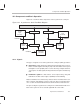

Table Of Contents
- Read This First
- Contents
- Figures
- Tables
- Examples
- Cautions
- Introduction
- Architectural Overview
- Central Processing Unit
- Memory and I/O Spaces
- Program Control
- Addressing Modes
- Assembly Language Instructions
- Instruction Set Summary
- How To Use the Instruction Descriptions
- Instruction Descriptions
- ABS
- ABS
- ADD
- ADD
- ADD
- ADD
- ADDC
- ADDC
- ADDS
- ADDS
- ADDT
- ADDT
- ADRK
- AND
- AND
- AND
- APAC
- APAC
- B
- BACC
- BANZ
- BANZ
- BCND
- BCND
- BIT
- BIT
- BITT
- BITT
- BLDD
- BLDD
- BLDD
- BLDD
- BLDD
- BLPD
- BLPD
- BLPD
- BLPD
- CALA
- CALL
- CC
- CC
- CLRC
- CLRC
- CMPL
- CMPR
- DMOV
- DMOV
- IDLE
- IN
- IN
- INTR
- LACC
- LACC
- LACC
- LACL
- LACL
- LACL
- LACT
- LACT
- LAR
- LAR
- LAR
- LDP
- LDP
- LPH
- LPH
- LST
- LST
- LST
- LST
- LT
- LT
- LTA
- LTA
- LTD
- LTD
- LTD
- LTP
- LTP
- LTS
- LTS
- MAC
- MAC
- MAC
- MAC
- MACD
- MACD
- MACD
- MACD
- MACD
- MAR
- MAR
- MPY
- MPY
- MPY
- MPYA
- MPYA
- MPYS
- MPYS
- MPYU
- MPYU
- NEG
- NEG
- NMI
- NOP
- NORM
- NORM
- NORM
- OR
- OR
- OR
- OUT
- OUT
- PAC
- POP
- POP
- POPD
- POPD
- PSHD
- PSHD
- PUSH
- RET
- RETC
- ROL
- ROR
- RPT
- RPT
- SACH
- SACH
- SACL
- SACL
- SAR
- SAR
- SBRK
- SETC
- SETC
- SFL
- SFR
- SFR
- SPAC
- SPH
- SPH
- SPL
- SPL
- SPLK
- SPLK
- SPM
- SQRA
- SQRA
- SQRS
- SQRS
- SST
- SST
- SUB
- SUB
- SUB
- SUB
- SUBB
- SUBB
- SUBC
- SUBC
- SUBS
- SUBS
- SUBT
- SUBT
- TBLR
- TBLR
- TBLR
- TBLW
- TBLW
- TBLW
- TRAP
- XOR
- XOR
- XOR
- ZALR
- ZALR
- On-Chip Peripherals
- Synchronous Serial Port
- Asynchronous Serial Port
- TMS320C209
- Register Summary
- TMS320C1x/C2x/C2xx/C5x Instruction Set Comparison
- Program Examples
- Submitting ROM Codes to TI
- Design Considerations for Using XDS510 Emulator
- E.1 Designing Your Target System’s Emulator Connector (14-Pin Header)
- E.2 Bus Protocol
- E.3 Emulator Cable Pod
- E.4 Emulator Cable Pod Signal Timing
- E.5 Emulation Timing Calculations
- E.6 Connections Between the Emulator and the Target System
- E.7 Physical Dimensions for the 14-Pin Emulator Connector
- E.8 Emulation Design Considerations
- Glossary
- Index

Controlling and Resetting the Port
10-8
Bits 12–10 Reserved. Always read as 0s.
Bit 9 DIM — Delta interrupt mask. DIM selects whether or not delta interrupts
are asserted on the TXRXINT interrupt line. A delta interrupt is generated by
a change on one of the general-purpose I/O pins (IO3, IO2, IO1, or IO0).
DIM = 0 Disables delta interrupts.
DIM = 1 Enables delta interrupts.
Bit 8 TIM — Transmit interrupt mask. TIM selects whether transmit interrupts
are asserted on the TXRXINT interrupt line. A transmit interrupt is generated
by THRE (transmit register empty indicator in the IOSR) when the transmit
register (ADTR) empties.
TIM = 0 Disables transmit interrupts.
TIM = 1 Enables transmit interrupts.
Bit 7 RIM — Receive interrupt mask. RIM selects whether receive interrupts are
asserted on the TXRXINT interrupt line. A receive interrupt is generated by
one of these indicators in the IOSR: BI (break interrupt), FE (framing error),
OE (overflow error), or DR (data ready).
RIM = 0 Disables receive interrupts.
RIM = 1 Enables receiver interrupts.
Bit 6 STB — Stop bit selector. STB selects the number of stop bits used in trans-
mission and reception.
STB = 0 One stop bit is used in transmission and reception. This is
the default value at reset.
STB = 1 Two stop bits are used in transmission and reception.
Bit 5 CAD — Calibrate
A
detect bit. CAD is used to enable and disable automatic
baud-rate alignment (auto-baud alignment).
CAD = 0 Disables auto-baud alignment.
CAD = 1 Enables auto-baud alignment.
Bit 4 SETBRK — Set break bit. Selects the output level of TX when the port is
not transmitting.
SETBRK = 0 The TX output is forced high when the port is not
transmitting.
SETBRK = 1 The TX output is forced low when the port is not
transmitting.