
User manual
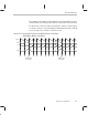
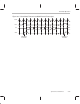
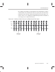
Table Of Contents
- Read This First
- Contents
- Figures
- Tables
- Examples
- Cautions
- Introduction
- Architectural Overview
- Central Processing Unit
- Memory and I/O Spaces
- Program Control
- Addressing Modes
- Assembly Language Instructions
- Instruction Set Summary
- How To Use the Instruction Descriptions
- Instruction Descriptions
- ABS
- ABS
- ADD
- ADD
- ADD
- ADD
- ADDC
- ADDC
- ADDS
- ADDS
- ADDT
- ADDT
- ADRK
- AND
- AND
- AND
- APAC
- APAC
- B
- BACC
- BANZ
- BANZ
- BCND
- BCND
- BIT
- BIT
- BITT
- BITT
- BLDD
- BLDD
- BLDD
- BLDD
- BLDD
- BLPD
- BLPD
- BLPD
- BLPD
- CALA
- CALL
- CC
- CC
- CLRC
- CLRC
- CMPL
- CMPR
- DMOV
- DMOV
- IDLE
- IN
- IN
- INTR
- LACC
- LACC
- LACC
- LACL
- LACL
- LACL
- LACT
- LACT
- LAR
- LAR
- LAR
- LDP
- LDP
- LPH
- LPH
- LST
- LST
- LST
- LST
- LT
- LT
- LTA
- LTA
- LTD
- LTD
- LTD
- LTP
- LTP
- LTS
- LTS
- MAC
- MAC
- MAC
- MAC
- MACD
- MACD
- MACD
- MACD
- MACD
- MAR
- MAR
- MPY
- MPY
- MPY
- MPYA
- MPYA
- MPYS
- MPYS
- MPYU
- MPYU
- NEG
- NEG
- NMI
- NOP
- NORM
- NORM
- NORM
- OR
- OR
- OR
- OUT
- OUT
- PAC
- POP
- POP
- POPD
- POPD
- PSHD
- PSHD
- PUSH
- RET
- RETC
- ROL
- ROR
- RPT
- RPT
- SACH
- SACH
- SACL
- SACL
- SAR
- SAR
- SBRK
- SETC
- SETC
- SFL
- SFR
- SFR
- SPAC
- SPH
- SPH
- SPL
- SPL
- SPLK
- SPLK
- SPM
- SQRA
- SQRA
- SQRS
- SQRS
- SST
- SST
- SUB
- SUB
- SUB
- SUB
- SUBB
- SUBB
- SUBC
- SUBC
- SUBS
- SUBS
- SUBT
- SUBT
- TBLR
- TBLR
- TBLR
- TBLW
- TBLW
- TBLW
- TRAP
- XOR
- XOR
- XOR
- ZALR
- ZALR
- On-Chip Peripherals
- Synchronous Serial Port
- Asynchronous Serial Port
- TMS320C209
- Register Summary
- TMS320C1x/C2x/C2xx/C5x Instruction Set Comparison
- Program Examples
- Submitting ROM Codes to TI
- Design Considerations for Using XDS510 Emulator
- E.1 Designing Your Target System’s Emulator Connector (14-Pin Header)
- E.2 Bus Protocol
- E.3 Emulator Cable Pod
- E.4 Emulator Cable Pod Signal Timing
- E.5 Emulation Timing Calculations
- E.6 Connections Between the Emulator and the Target System
- E.7 Physical Dimensions for the 14-Pin Emulator Connector
- E.8 Emulation Design Considerations
- Glossary
- Index

Transmitter Operation
9-22
9.5.4 Continuous Mode Transmission with External Frame Sync (FSM=0, TXM=0)
Use continuous mode transmission with external frame sync to transfer long
packets at maximum packet frequency while using an external frame sync
generator. Place the transmitter in continuous mode with external frame sync
by setting the FSM bit to 0 and the TXM bit to 0.
In continuous mode, frame sync pulses are not necessary after the initial pulse
for consecutive packet transfers. A frame sync is generated only for the first
transmission. As long as the FIFO buffer has new values to transmit, the mode
continues. Transmission halts when the buffer empties. If SDTR is written to
after the halt, the device starts a new continuous mode transmission.
This mode of operation offers several features:
Only one frame sync is necessary for the transmission of consecutive
packets.
If the FIFO buffer is not empty, the mode continues. If the FIFO buffer is
empty, the process ends.
Generally, the transmit clock and the receive clock have the same source. This
allows each bit to be transmitted from another device on a rising edge of the
clock signal and received by the ’C2xx on the next falling edge of the clock sig-
nal.
Continuous mode transmission with external frame sync requires the following
order of events (see Figure 9–7):
1) A frame sync pulse initiates the transmission. The pulse is sampled on the
falling edge of CLKX. After the falling edge of CLKX, the contents of the
current word in the transmit FIFO buffer are transferred to the XSR. If the
FIFO buffer becomes empty during this operation, then it generates a
XINT to request more data.
2) On the next rising edge of CLKX after FSX goes high, DX is driven with
the first bit (MSB) of the word to be transmitted.
3) The frame sync goes low (and remains low during word transmission).
4) Once FSX goes low, the rest of the bits are shifted out.
5) Once the entire word in the XSR is shifted out, the next word is loaded in
and the first bit of the word is placed on the DX pin. Then, the process re-
peats beginning with step four. If a new word is not in the transmit FIFO
buffer, then the process ends.
If the SDTR is loaded with a new word while the transmit FIFO buffer is full, the
new word will be lost; the FIFO buffer will not accept any more than four words.