
User manual
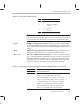
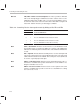
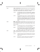
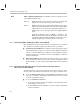
Table Of Contents
- Read This First
- Contents
- Figures
- Tables
- Examples
- Cautions
- Introduction
- Architectural Overview
- Central Processing Unit
- Memory and I/O Spaces
- Program Control
- Addressing Modes
- Assembly Language Instructions
- Instruction Set Summary
- How To Use the Instruction Descriptions
- Instruction Descriptions
- ABS
- ABS
- ADD
- ADD
- ADD
- ADD
- ADDC
- ADDC
- ADDS
- ADDS
- ADDT
- ADDT
- ADRK
- AND
- AND
- AND
- APAC
- APAC
- B
- BACC
- BANZ
- BANZ
- BCND
- BCND
- BIT
- BIT
- BITT
- BITT
- BLDD
- BLDD
- BLDD
- BLDD
- BLDD
- BLPD
- BLPD
- BLPD
- BLPD
- CALA
- CALL
- CC
- CC
- CLRC
- CLRC
- CMPL
- CMPR
- DMOV
- DMOV
- IDLE
- IN
- IN
- INTR
- LACC
- LACC
- LACC
- LACL
- LACL
- LACL
- LACT
- LACT
- LAR
- LAR
- LAR
- LDP
- LDP
- LPH
- LPH
- LST
- LST
- LST
- LST
- LT
- LT
- LTA
- LTA
- LTD
- LTD
- LTD
- LTP
- LTP
- LTS
- LTS
- MAC
- MAC
- MAC
- MAC
- MACD
- MACD
- MACD
- MACD
- MACD
- MAR
- MAR
- MPY
- MPY
- MPY
- MPYA
- MPYA
- MPYS
- MPYS
- MPYU
- MPYU
- NEG
- NEG
- NMI
- NOP
- NORM
- NORM
- NORM
- OR
- OR
- OR
- OUT
- OUT
- PAC
- POP
- POP
- POPD
- POPD
- PSHD
- PSHD
- PUSH
- RET
- RETC
- ROL
- ROR
- RPT
- RPT
- SACH
- SACH
- SACL
- SACL
- SAR
- SAR
- SBRK
- SETC
- SETC
- SFL
- SFR
- SFR
- SPAC
- SPH
- SPH
- SPL
- SPL
- SPLK
- SPLK
- SPM
- SQRA
- SQRA
- SQRS
- SQRS
- SST
- SST
- SUB
- SUB
- SUB
- SUB
- SUBB
- SUBB
- SUBC
- SUBC
- SUBS
- SUBS
- SUBT
- SUBT
- TBLR
- TBLR
- TBLR
- TBLW
- TBLW
- TBLW
- TRAP
- XOR
- XOR
- XOR
- ZALR
- ZALR
- On-Chip Peripherals
- Synchronous Serial Port
- Asynchronous Serial Port
- TMS320C209
- Register Summary
- TMS320C1x/C2x/C2xx/C5x Instruction Set Comparison
- Program Examples
- Submitting ROM Codes to TI
- Design Considerations for Using XDS510 Emulator
- E.1 Designing Your Target System’s Emulator Connector (14-Pin Header)
- E.2 Bus Protocol
- E.3 Emulator Cable Pod
- E.4 Emulator Cable Pod Signal Timing
- E.5 Emulation Timing Calculations
- E.6 Connections Between the Emulator and the Target System
- E.7 Physical Dimensions for the 14-Pin Emulator Connector
- E.8 Emulation Design Considerations
- Glossary
- Index

Controlling and Resetting the Port
9-9
Synchronous Serial Port
Table 9–2. Run and Emulation Modes
FREE SOFT Run/Emulation Mode
0 0 Immediate stop
0 1 Stop after completion
of word
1 0 Free run
1 1 Free run
Note:
If an option besides immediate stop is chosen for the receiver, an overflow
error is possible. The default mode (selected at reset) is
immediate stop.
Bit 13 TCOMP — Transmission complete. This bit is cleared to 0 when all data
in the transmit FIFO buffer has been transmitted (the buffer is empty) and is
set to 1 when new data is written to the transmit FIFO buffer (the buffer is not
empty).
Bit 12 RFNE — Receive FIFO buffer not empty bit. This bit is 1 when the receive
FIFO buffer contains data and is cleared when the buffer empties.
Bits 11–10 FT1, FT0 — FIFO transmit-interrupt bits. The values you write to FT0 and
FT1 set an interrupt trigger condition based on the contents of the transmit
FIFO buffer. When this condition is met, a transmit interrupt (XINT) is gener-
ated and the data can be transferred out to the FIFO buffer using the OUT
instruction. Table 9–3 summarizes the possible trigger conditions.
Table 9–3. Controlling Transmit Interrupt Generation by Writing to Bits FT1 and FT0
Select Bits
FT1 FT0 Generate XINT when...
0 0 Transmit FIFO buffer can accept one or more words;
XINT occurs repeatedly until the buffer is full.
0 1 Transmit FIFO buffer can accept two or more words;
XINT occurs repeatedly until three words are written.
1 0 Transmit FIFO buffer can accept three or four words;
XINT occurs repeatedly until two words are written.
1 1 Transmit FIFO buffer is empty (can accept 4 words);
XINT occurs repeatedly until one word is written.