
User manual
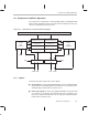
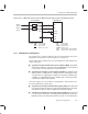
Table Of Contents
- Read This First
- Contents
- Figures
- Tables
- Examples
- Cautions
- Introduction
- Architectural Overview
- Central Processing Unit
- Memory and I/O Spaces
- Program Control
- Addressing Modes
- Assembly Language Instructions
- Instruction Set Summary
- How To Use the Instruction Descriptions
- Instruction Descriptions
- ABS
- ABS
- ADD
- ADD
- ADD
- ADD
- ADDC
- ADDC
- ADDS
- ADDS
- ADDT
- ADDT
- ADRK
- AND
- AND
- AND
- APAC
- APAC
- B
- BACC
- BANZ
- BANZ
- BCND
- BCND
- BIT
- BIT
- BITT
- BITT
- BLDD
- BLDD
- BLDD
- BLDD
- BLDD
- BLPD
- BLPD
- BLPD
- BLPD
- CALA
- CALL
- CC
- CC
- CLRC
- CLRC
- CMPL
- CMPR
- DMOV
- DMOV
- IDLE
- IN
- IN
- INTR
- LACC
- LACC
- LACC
- LACL
- LACL
- LACL
- LACT
- LACT
- LAR
- LAR
- LAR
- LDP
- LDP
- LPH
- LPH
- LST
- LST
- LST
- LST
- LT
- LT
- LTA
- LTA
- LTD
- LTD
- LTD
- LTP
- LTP
- LTS
- LTS
- MAC
- MAC
- MAC
- MAC
- MACD
- MACD
- MACD
- MACD
- MACD
- MAR
- MAR
- MPY
- MPY
- MPY
- MPYA
- MPYA
- MPYS
- MPYS
- MPYU
- MPYU
- NEG
- NEG
- NMI
- NOP
- NORM
- NORM
- NORM
- OR
- OR
- OR
- OUT
- OUT
- PAC
- POP
- POP
- POPD
- POPD
- PSHD
- PSHD
- PUSH
- RET
- RETC
- ROL
- ROR
- RPT
- RPT
- SACH
- SACH
- SACL
- SACL
- SAR
- SAR
- SBRK
- SETC
- SETC
- SFL
- SFR
- SFR
- SPAC
- SPH
- SPH
- SPL
- SPL
- SPLK
- SPLK
- SPM
- SQRA
- SQRA
- SQRS
- SQRS
- SST
- SST
- SUB
- SUB
- SUB
- SUB
- SUBB
- SUBB
- SUBC
- SUBC
- SUBS
- SUBS
- SUBT
- SUBT
- TBLR
- TBLR
- TBLR
- TBLW
- TBLW
- TBLW
- TRAP
- XOR
- XOR
- XOR
- ZALR
- ZALR
- On-Chip Peripherals
- Synchronous Serial Port
- Asynchronous Serial Port
- TMS320C209
- Register Summary
- TMS320C1x/C2x/C2xx/C5x Instruction Set Comparison
- Program Examples
- Submitting ROM Codes to TI
- Design Considerations for Using XDS510 Emulator
- E.1 Designing Your Target System’s Emulator Connector (14-Pin Header)
- E.2 Bus Protocol
- E.3 Emulator Cable Pod
- E.4 Emulator Cable Pod Signal Timing
- E.5 Emulation Timing Calculations
- E.6 Connections Between the Emulator and the Target System
- E.7 Physical Dimensions for the 14-Pin Emulator Connector
- E.8 Emulation Design Considerations
- Glossary
- Index

Components and Basic Operation
9-7
Synchronous Serial Port
Receiving a word through the serial port typically is done as follows:
1) Data from the DR pin is shifted, bit-by-bit (MSB first), into the receive shift
register (RSR).
2) When the RSR is full, the RSR copies the data to the receive FIFO buffer.
3) The process then does one of two things, depending upon the state of the
receive FIFO buffer:
If the receive FIFO buffer is not full, the process repeats from step 1.
If the receive FIFO buffer is full (as specified by the FR1 and FR0 bits in
the SSPCR), it sends a receive interrupt (RINT) to the processor to re-
quest servicing.
4) The processor can read the received data from the receive FIFO buffer
through the SDTR.