
User manual
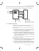
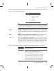
Table Of Contents
- Read This First
- Contents
- Figures
- Tables
- Examples
- Cautions
- Introduction
- Architectural Overview
- Central Processing Unit
- Memory and I/O Spaces
- Program Control
- Addressing Modes
- Assembly Language Instructions
- Instruction Set Summary
- How To Use the Instruction Descriptions
- Instruction Descriptions
- ABS
- ABS
- ADD
- ADD
- ADD
- ADD
- ADDC
- ADDC
- ADDS
- ADDS
- ADDT
- ADDT
- ADRK
- AND
- AND
- AND
- APAC
- APAC
- B
- BACC
- BANZ
- BANZ
- BCND
- BCND
- BIT
- BIT
- BITT
- BITT
- BLDD
- BLDD
- BLDD
- BLDD
- BLDD
- BLPD
- BLPD
- BLPD
- BLPD
- CALA
- CALL
- CC
- CC
- CLRC
- CLRC
- CMPL
- CMPR
- DMOV
- DMOV
- IDLE
- IN
- IN
- INTR
- LACC
- LACC
- LACC
- LACL
- LACL
- LACL
- LACT
- LACT
- LAR
- LAR
- LAR
- LDP
- LDP
- LPH
- LPH
- LST
- LST
- LST
- LST
- LT
- LT
- LTA
- LTA
- LTD
- LTD
- LTD
- LTP
- LTP
- LTS
- LTS
- MAC
- MAC
- MAC
- MAC
- MACD
- MACD
- MACD
- MACD
- MACD
- MAR
- MAR
- MPY
- MPY
- MPY
- MPYA
- MPYA
- MPYS
- MPYS
- MPYU
- MPYU
- NEG
- NEG
- NMI
- NOP
- NORM
- NORM
- NORM
- OR
- OR
- OR
- OUT
- OUT
- PAC
- POP
- POP
- POPD
- POPD
- PSHD
- PSHD
- PUSH
- RET
- RETC
- ROL
- ROR
- RPT
- RPT
- SACH
- SACH
- SACL
- SACL
- SAR
- SAR
- SBRK
- SETC
- SETC
- SFL
- SFR
- SFR
- SPAC
- SPH
- SPH
- SPL
- SPL
- SPLK
- SPLK
- SPM
- SQRA
- SQRA
- SQRS
- SQRS
- SST
- SST
- SUB
- SUB
- SUB
- SUB
- SUBB
- SUBB
- SUBC
- SUBC
- SUBS
- SUBS
- SUBT
- SUBT
- TBLR
- TBLR
- TBLR
- TBLW
- TBLW
- TBLW
- TRAP
- XOR
- XOR
- XOR
- ZALR
- ZALR
- On-Chip Peripherals
- Synchronous Serial Port
- Asynchronous Serial Port
- TMS320C209
- Register Summary
- TMS320C1x/C2x/C2xx/C5x Instruction Set Comparison
- Program Examples
- Submitting ROM Codes to TI
- Design Considerations for Using XDS510 Emulator
- E.1 Designing Your Target System’s Emulator Connector (14-Pin Header)
- E.2 Bus Protocol
- E.3 Emulator Cable Pod
- E.4 Emulator Cable Pod Signal Timing
- E.5 Emulation Timing Calculations
- E.6 Connections Between the Emulator and the Target System
- E.7 Physical Dimensions for the 14-Pin Emulator Connector
- E.8 Emulation Design Considerations
- Glossary
- Index
Components and Basic Operation
9-5
Synchronous Serial Port
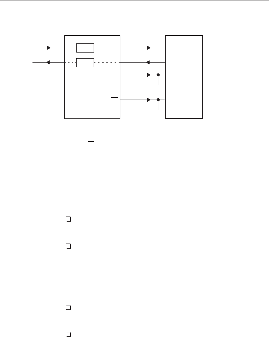
Figure 9–2. 2-Way Serial Port Transfer With External Frame Sync and External Clock
TMS320C203
TLC320AD55C
Analog
signal
A/D
D/A
Analog
signal
DR
DX
CLKX
CLKR
FSX
FSR
D
OUT
D
IN
SCK
FS
Legend: D
OUT
Transmit data DR Receive data
D
IN
Receive data DX Transmit data
SCK Clock source CLKX Transmit clock
FS
Frame sync source CLKR Receive clock
FSX Transmit frame synchronization
FSR Receive frame synchronization
9.2.2 FIFO Buffers and Registers
The synchronous serial port (SSP) has two four-level transmit and receive
FIFO buffers (shown at the center of Figure 9–1 on page 9-3).
Two on-chip registers allow you to access the FIFO buffers and control the op-
eration of the port:
Synchronous data transmit and receive register (SDTR). The SDTR,
at I/O address FFF0h, is used for the top of both FIFO buffers (transmit and
receive) and is the only visible part of the FIFO buffers.
Synchronous serial port control register (SSPCR). The SSPCR, at I/O
address FFF1h, contains bits for setting port modes, indicating the status
of a data transfer, setting trigger conditions for interrupts, indicating error
conditions, accepting bit input, and resetting the port. Section 9.3 includes
a detailed description of the SSPCR.
Two other registers (not accessible to a programmer) control transfers be-
tween the FIFO buffers and the pins:
Synchronous serial port transmit shift register (XSR). Each data word
is transferred from the bottom level of the transmit FIFO buffer to the XSR.
The XSR then shifts the data out (MSB first) through the DX pin.
Synchronous serial port receive shift register (RSR). Each data word
is accepted, one bit at a time, at the DR pin and shifted into the RSR. The
RSR then transfers the word to the bottom level of the receive FIFO buffer.