
User manual
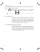
Table Of Contents
- Read This First
- Contents
- Figures
- Tables
- Examples
- Cautions
- Introduction
- Architectural Overview
- Central Processing Unit
- Memory and I/O Spaces
- Program Control
- Addressing Modes
- Assembly Language Instructions
- Instruction Set Summary
- How To Use the Instruction Descriptions
- Instruction Descriptions
- ABS
- ABS
- ADD
- ADD
- ADD
- ADD
- ADDC
- ADDC
- ADDS
- ADDS
- ADDT
- ADDT
- ADRK
- AND
- AND
- AND
- APAC
- APAC
- B
- BACC
- BANZ
- BANZ
- BCND
- BCND
- BIT
- BIT
- BITT
- BITT
- BLDD
- BLDD
- BLDD
- BLDD
- BLDD
- BLPD
- BLPD
- BLPD
- BLPD
- CALA
- CALL
- CC
- CC
- CLRC
- CLRC
- CMPL
- CMPR
- DMOV
- DMOV
- IDLE
- IN
- IN
- INTR
- LACC
- LACC
- LACC
- LACL
- LACL
- LACL
- LACT
- LACT
- LAR
- LAR
- LAR
- LDP
- LDP
- LPH
- LPH
- LST
- LST
- LST
- LST
- LT
- LT
- LTA
- LTA
- LTD
- LTD
- LTD
- LTP
- LTP
- LTS
- LTS
- MAC
- MAC
- MAC
- MAC
- MACD
- MACD
- MACD
- MACD
- MACD
- MAR
- MAR
- MPY
- MPY
- MPY
- MPYA
- MPYA
- MPYS
- MPYS
- MPYU
- MPYU
- NEG
- NEG
- NMI
- NOP
- NORM
- NORM
- NORM
- OR
- OR
- OR
- OUT
- OUT
- PAC
- POP
- POP
- POPD
- POPD
- PSHD
- PSHD
- PUSH
- RET
- RETC
- ROL
- ROR
- RPT
- RPT
- SACH
- SACH
- SACL
- SACL
- SAR
- SAR
- SBRK
- SETC
- SETC
- SFL
- SFR
- SFR
- SPAC
- SPH
- SPH
- SPL
- SPL
- SPLK
- SPLK
- SPM
- SQRA
- SQRA
- SQRS
- SQRS
- SST
- SST
- SUB
- SUB
- SUB
- SUB
- SUBB
- SUBB
- SUBC
- SUBC
- SUBS
- SUBS
- SUBT
- SUBT
- TBLR
- TBLR
- TBLR
- TBLW
- TBLW
- TBLW
- TRAP
- XOR
- XOR
- XOR
- ZALR
- ZALR
- On-Chip Peripherals
- Synchronous Serial Port
- Asynchronous Serial Port
- TMS320C209
- Register Summary
- TMS320C1x/C2x/C2xx/C5x Instruction Set Comparison
- Program Examples
- Submitting ROM Codes to TI
- Design Considerations for Using XDS510 Emulator
- E.1 Designing Your Target System’s Emulator Connector (14-Pin Header)
- E.2 Bus Protocol
- E.3 Emulator Cable Pod
- E.4 Emulator Cable Pod Signal Timing
- E.5 Emulation Timing Calculations
- E.6 Connections Between the Emulator and the Target System
- E.7 Physical Dimensions for the 14-Pin Emulator Connector
- E.8 Emulation Design Considerations
- Glossary
- Index

General-Purpose I/O Pins
8-17
On-Chip Peripherals
8.6 General-Purpose I/O Pins
The ’C2xx provides pins that can be used to supply input signals from an exter-
nal device or output signals to an external device. These pins are not bound
to specific uses; rather, they can provide input or output signals for a great vari-
ety purposes. You have access to the general-purpose input pin BIO
and the
general-purpose output pin XF. On ’C2xx devices other than the ’C209, you
also have the pins IO0, IO1, IO2, and IO3, which can each be configured as
an input pin or an output pin.
8.6.1 Input Pin BIO
The general-purpose input pin BIO pin provides input from an external device
and is particularly helpful as an alternative to an interrupt when time-critical
loops must not be disturbed. The BIO
signal gives you control through three
instructions, a conditional branch (BCND), a conditional call (CC), and a condi-
tional return (RETC). Here is an example of each:
BCND
pma
, BIO
pma
is a program memory address that you specify. The CPU branches to
the program memory address if BIO
is low.
CC
pma
, BIO
pma
is a program memory address that you specify. If BIO is low, the CPU
stores the return address to the top of the hardware stack and then
branches to the program memory address.
RETC BIO
If BIO
is low, the CPU transfers the return address from the stack to the
program counter (PC) to return from a subroutine or interrupt service rou-
tine.
If BIO
is not used, it should be pulled high so that a conditional branch, call,
or return will not be executed accidentally.
An example of BIO
timing is shown in Figure 8–7. This timing diagram is for
a sequence of single-cycle, single-word instructions located in external
memory. BIO
must be asserted low for at least one CLKOUT1 cycle. The
BCND, CC, and RETC instructions sample the BIO
pin during their execute
phase in the pipeline. Actual timing may vary with different instruction se-
quences.