
User manual
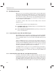
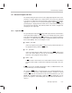
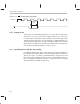
Table Of Contents
- Read This First
- Contents
- Figures
- Tables
- Examples
- Cautions
- Introduction
- Architectural Overview
- Central Processing Unit
- Memory and I/O Spaces
- Program Control
- Addressing Modes
- Assembly Language Instructions
- Instruction Set Summary
- How To Use the Instruction Descriptions
- Instruction Descriptions
- ABS
- ABS
- ADD
- ADD
- ADD
- ADD
- ADDC
- ADDC
- ADDS
- ADDS
- ADDT
- ADDT
- ADRK
- AND
- AND
- AND
- APAC
- APAC
- B
- BACC
- BANZ
- BANZ
- BCND
- BCND
- BIT
- BIT
- BITT
- BITT
- BLDD
- BLDD
- BLDD
- BLDD
- BLDD
- BLPD
- BLPD
- BLPD
- BLPD
- CALA
- CALL
- CC
- CC
- CLRC
- CLRC
- CMPL
- CMPR
- DMOV
- DMOV
- IDLE
- IN
- IN
- INTR
- LACC
- LACC
- LACC
- LACL
- LACL
- LACL
- LACT
- LACT
- LAR
- LAR
- LAR
- LDP
- LDP
- LPH
- LPH
- LST
- LST
- LST
- LST
- LT
- LT
- LTA
- LTA
- LTD
- LTD
- LTD
- LTP
- LTP
- LTS
- LTS
- MAC
- MAC
- MAC
- MAC
- MACD
- MACD
- MACD
- MACD
- MACD
- MAR
- MAR
- MPY
- MPY
- MPY
- MPYA
- MPYA
- MPYS
- MPYS
- MPYU
- MPYU
- NEG
- NEG
- NMI
- NOP
- NORM
- NORM
- NORM
- OR
- OR
- OR
- OUT
- OUT
- PAC
- POP
- POP
- POPD
- POPD
- PSHD
- PSHD
- PUSH
- RET
- RETC
- ROL
- ROR
- RPT
- RPT
- SACH
- SACH
- SACL
- SACL
- SAR
- SAR
- SBRK
- SETC
- SETC
- SFL
- SFR
- SFR
- SPAC
- SPH
- SPH
- SPL
- SPL
- SPLK
- SPLK
- SPM
- SQRA
- SQRA
- SQRS
- SQRS
- SST
- SST
- SUB
- SUB
- SUB
- SUB
- SUBB
- SUBB
- SUBC
- SUBC
- SUBS
- SUBS
- SUBT
- SUBT
- TBLR
- TBLR
- TBLR
- TBLW
- TBLW
- TBLW
- TRAP
- XOR
- XOR
- XOR
- ZALR
- ZALR
- On-Chip Peripherals
- Synchronous Serial Port
- Asynchronous Serial Port
- TMS320C209
- Register Summary
- TMS320C1x/C2x/C2xx/C5x Instruction Set Comparison
- Program Examples
- Submitting ROM Codes to TI
- Design Considerations for Using XDS510 Emulator
- E.1 Designing Your Target System’s Emulator Connector (14-Pin Header)
- E.2 Bus Protocol
- E.3 Emulator Cable Pod
- E.4 Emulator Cable Pod Signal Timing
- E.5 Emulation Timing Calculations
- E.6 Connections Between the Emulator and the Target System
- E.7 Physical Dimensions for the 14-Pin Emulator Connector
- E.8 Emulation Design Considerations
- Glossary
- Index
Wait-State Generator
8-16
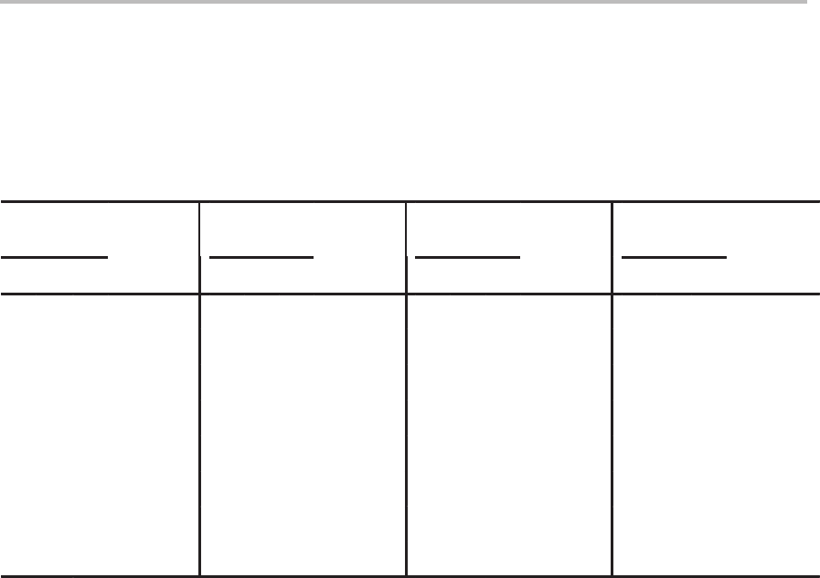
Table 8–4 shows how to set the number of wait states you want for each type
of off-chip memory. For example, if you write 1s to bits 0 through 5, the device
will generate seven wait states for off-chip lower program memory and seven
wait states for off-chip upper program memory.
Table 8–4. Setting the Number of Wait States With the ’C2xx WSGR Bits
ISWS Bits
I/O Wait
DSWS Bits
Data Wait
PSUWS
Bits
Upper
Program
Wait
PSLWS
Bits
Lower
Program
Wait
11 10 9
I/O
W
a
it
States
8 7 6
D
a
t
a
W
a
it
States
5 4 3
W
a
it
States
2 1 0
W
a
it
States
0 0 0 0 0 0 0 0 0 0 0 0 0 0 0 0
0 0 1 1 0 0 1 1 0 0 1 1 0 0 1 1
0 1 0 2 0 1 0 2 0 1 0 2 0 1 0 2
0 1 1 3 0 1 1 3 0 1 1 3 0 1 1 3
1 0 0 4 1 0 0 4 1 0 0 4 1 0 0 4
1 0 1 5 1 0 1 5 1 0 1 5 1 0 1 5
1 1 0 6 1 1 0 6 1 1 0 6 1 1 0 6
1 1 1 7 1 1 1 7 1 1 1 7 1 1 1 7
In summary, the wait-state generator inserts zero to seven wait states to a giv-
en memory space, depending on the values of PSLWS, PSUWS, DSWS, and
ISWS, while the READY signal remains high. The READY signal may then be
driven low to generate additional wait states. If
m
is the number of CLKOUT1
cycles required for a particular read or write operation and
w
is the number of
wait states added, the operation will take (
m
+
w
) cycles. At reset, all WSGR
bits are set to 1, making seven wait states the default for every memory space.