
User manual
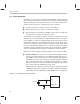
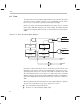
Table Of Contents
- Read This First
- Contents
- Figures
- Tables
- Examples
- Cautions
- Introduction
- Architectural Overview
- Central Processing Unit
- Memory and I/O Spaces
- Program Control
- Addressing Modes
- Assembly Language Instructions
- Instruction Set Summary
- How To Use the Instruction Descriptions
- Instruction Descriptions
- ABS
- ABS
- ADD
- ADD
- ADD
- ADD
- ADDC
- ADDC
- ADDS
- ADDS
- ADDT
- ADDT
- ADRK
- AND
- AND
- AND
- APAC
- APAC
- B
- BACC
- BANZ
- BANZ
- BCND
- BCND
- BIT
- BIT
- BITT
- BITT
- BLDD
- BLDD
- BLDD
- BLDD
- BLDD
- BLPD
- BLPD
- BLPD
- BLPD
- CALA
- CALL
- CC
- CC
- CLRC
- CLRC
- CMPL
- CMPR
- DMOV
- DMOV
- IDLE
- IN
- IN
- INTR
- LACC
- LACC
- LACC
- LACL
- LACL
- LACL
- LACT
- LACT
- LAR
- LAR
- LAR
- LDP
- LDP
- LPH
- LPH
- LST
- LST
- LST
- LST
- LT
- LT
- LTA
- LTA
- LTD
- LTD
- LTD
- LTP
- LTP
- LTS
- LTS
- MAC
- MAC
- MAC
- MAC
- MACD
- MACD
- MACD
- MACD
- MACD
- MAR
- MAR
- MPY
- MPY
- MPY
- MPYA
- MPYA
- MPYS
- MPYS
- MPYU
- MPYU
- NEG
- NEG
- NMI
- NOP
- NORM
- NORM
- NORM
- OR
- OR
- OR
- OUT
- OUT
- PAC
- POP
- POP
- POPD
- POPD
- PSHD
- PSHD
- PUSH
- RET
- RETC
- ROL
- ROR
- RPT
- RPT
- SACH
- SACH
- SACL
- SACL
- SAR
- SAR
- SBRK
- SETC
- SETC
- SFL
- SFR
- SFR
- SPAC
- SPH
- SPH
- SPL
- SPL
- SPLK
- SPLK
- SPM
- SQRA
- SQRA
- SQRS
- SQRS
- SST
- SST
- SUB
- SUB
- SUB
- SUB
- SUBB
- SUBB
- SUBC
- SUBC
- SUBS
- SUBS
- SUBT
- SUBT
- TBLR
- TBLR
- TBLR
- TBLW
- TBLW
- TBLW
- TRAP
- XOR
- XOR
- XOR
- ZALR
- ZALR
- On-Chip Peripherals
- Synchronous Serial Port
- Asynchronous Serial Port
- TMS320C209
- Register Summary
- TMS320C1x/C2x/C2xx/C5x Instruction Set Comparison
- Program Examples
- Submitting ROM Codes to TI
- Design Considerations for Using XDS510 Emulator
- E.1 Designing Your Target System’s Emulator Connector (14-Pin Header)
- E.2 Bus Protocol
- E.3 Emulator Cable Pod
- E.4 Emulator Cable Pod Signal Timing
- E.5 Emulation Timing Calculations
- E.6 Connections Between the Emulator and the Target System
- E.7 Physical Dimensions for the 14-Pin Emulator Connector
- E.8 Emulation Design Considerations
- Glossary
- Index
Clock Generator
8-5
On-Chip Peripherals
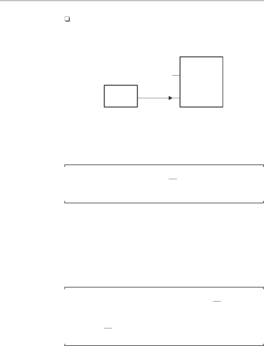
External Oscillator. CLKIN is the output of an external oscillator, which
is connected to the CLKIN/X2 pin. The X1 pin must be left unconnected.
See Figure 8–2.
Figure 8–2. Using an External Oscillator
’C2xx
X1
CLKIN/X2
No connection
Oscillator
Regardless of the method used to generate CLKOUT1, CLKOUT1 is also
available at the CLKOUT1 pin, unless the pin is turned off by the CLK register
(see Section 8.3).
You can lower the power requirements for the ’C2xx by slowing down or stop-
ping the input clock.
Note:
When restarting the system, activate RS
before starting or stopping the
clock, and hold it active until the clock stabilizes. This brings the device back
to a known state.
8.2.1 Clock Generator Options
The ’C2xx provides four clock modes: divide-by-2 (÷2), multiply-by-1 (×1),
multiply-by-2 (×2), and multiply-by-4 (×4). The
÷2 mode operates the CPU at
half the input clock rate. Each of the other modes operates the CPU at a multi-
ple of the input clock rate and phase locks the output clock with the the input
clock. You set the mode by changing the levels on the DIV1 and DIV2 pins. For
each mode, Table 8–2 shows the generated CPU clock rate and the state of
DIV2, DIV1, the internal oscillator, and the internal phase lock loop (PLL).
Notes:
1) Change DIV1 and DIV2 only while the reset signal (RS
) is active.
2) The PLL requires approximately 2500 cycles to lock the output clock sig-
nal to the input clock signal. When setting the ×1, ×2, or ×4 mode, keep
the reset (RS) signal active until at least three cycles after the PLL has
stabilized.