
User manual
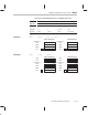


Table Of Contents
- Read This First
- Contents
- Figures
- Tables
- Examples
- Cautions
- Introduction
- Architectural Overview
- Central Processing Unit
- Memory and I/O Spaces
- Program Control
- Addressing Modes
- Assembly Language Instructions
- Instruction Set Summary
- How To Use the Instruction Descriptions
- Instruction Descriptions
- ABS
- ABS
- ADD
- ADD
- ADD
- ADD
- ADDC
- ADDC
- ADDS
- ADDS
- ADDT
- ADDT
- ADRK
- AND
- AND
- AND
- APAC
- APAC
- B
- BACC
- BANZ
- BANZ
- BCND
- BCND
- BIT
- BIT
- BITT
- BITT
- BLDD
- BLDD
- BLDD
- BLDD
- BLDD
- BLPD
- BLPD
- BLPD
- BLPD
- CALA
- CALL
- CC
- CC
- CLRC
- CLRC
- CMPL
- CMPR
- DMOV
- DMOV
- IDLE
- IN
- IN
- INTR
- LACC
- LACC
- LACC
- LACL
- LACL
- LACL
- LACT
- LACT
- LAR
- LAR
- LAR
- LDP
- LDP
- LPH
- LPH
- LST
- LST
- LST
- LST
- LT
- LT
- LTA
- LTA
- LTD
- LTD
- LTD
- LTP
- LTP
- LTS
- LTS
- MAC
- MAC
- MAC
- MAC
- MACD
- MACD
- MACD
- MACD
- MACD
- MAR
- MAR
- MPY
- MPY
- MPY
- MPYA
- MPYA
- MPYS
- MPYS
- MPYU
- MPYU
- NEG
- NEG
- NMI
- NOP
- NORM
- NORM
- NORM
- OR
- OR
- OR
- OUT
- OUT
- PAC
- POP
- POP
- POPD
- POPD
- PSHD
- PSHD
- PUSH
- RET
- RETC
- ROL
- ROR
- RPT
- RPT
- SACH
- SACH
- SACL
- SACL
- SAR
- SAR
- SBRK
- SETC
- SETC
- SFL
- SFR
- SFR
- SPAC
- SPH
- SPH
- SPL
- SPL
- SPLK
- SPLK
- SPM
- SQRA
- SQRA
- SQRS
- SQRS
- SST
- SST
- SUB
- SUB
- SUB
- SUB
- SUBB
- SUBB
- SUBC
- SUBC
- SUBS
- SUBS
- SUBT
- SUBT
- TBLR
- TBLR
- TBLR
- TBLW
- TBLW
- TBLW
- TRAP
- XOR
- XOR
- XOR
- ZALR
- ZALR
- On-Chip Peripherals
- Synchronous Serial Port
- Asynchronous Serial Port
- TMS320C209
- Register Summary
- TMS320C1x/C2x/C2xx/C5x Instruction Set Comparison
- Program Examples
- Submitting ROM Codes to TI
- Design Considerations for Using XDS510 Emulator
- E.1 Designing Your Target System’s Emulator Connector (14-Pin Header)
- E.2 Bus Protocol
- E.3 Emulator Cable Pod
- E.4 Emulator Cable Pod Signal Timing
- E.5 Emulation Timing Calculations
- E.6 Connections Between the Emulator and the Target System
- E.7 Physical Dimensions for the 14-Pin Emulator Connector
- E.8 Emulation Design Considerations
- Glossary
- Index
MPYU
Multiply Unsigned
7-120
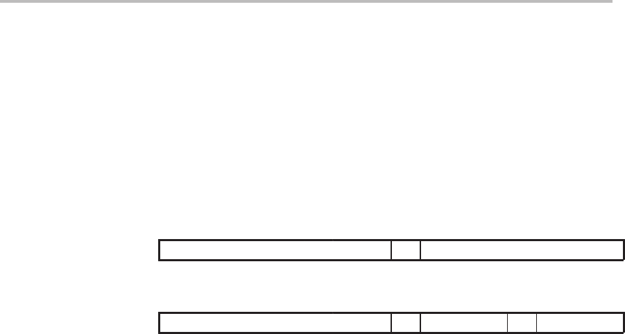
Syntax MPYU
dma
Direct addressing
MPYU
ind
[, AR
n
] Indirect addressing
Operands dma: 7 LSBs of the data-memory address
n: Value from 0 to 7 designating the next auxiliary register
ind: Select one of the following seven options:
* *+ *– *0+ *0– *BR0+ *BR0–
MPYU
dma
1514131211109876543210
0
10101010 dma
MPYU
ind
[,AR
n
]
1514131211109876543210
0
10101011 ARU N NAR
Note: ARU, N, and NAR are defined in Section 6.3,
Indirect Addressing Mode
(page 6-9).
Execution Increment PC, then ...
Unsigned (TREG) × unsigned (data-memory address) → PREG
Status Bits None
This instruction is not affected by SXM.
Description The unsigned contents of TREG are multiplied by the unsigned contents of the
addressed data-memory location. The result is placed in the product register
(PREG). The multiplier acts as a signed 17 × 17-bit multiplier for this instruc-
tion, with the MSB of both operands forced to 0.
When another instruction passes the resulting PREG value to data memory
or to the CALU, the value passes first through the product shifter at the output
of the PREG. This shifter always invokes sign extension on the PREG value
when PM = 3 (right-shift-by-6 mode). Therefore, this shift mode should not be
used if unsigned products are desired.
The MPYU instruction is particularly useful for computing multiple-precision
products, such as when multiplying two 32-bit numbers to yield a 64-bit prod-
uct.
Words 1
Opcode