
User manual
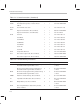
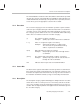
Table Of Contents
- Read This First
- Contents
- Figures
- Tables
- Examples
- Cautions
- Introduction
- Architectural Overview
- Central Processing Unit
- Memory and I/O Spaces
- Program Control
- Addressing Modes
- Assembly Language Instructions
- Instruction Set Summary
- How To Use the Instruction Descriptions
- Instruction Descriptions
- ABS
- ABS
- ADD
- ADD
- ADD
- ADD
- ADDC
- ADDC
- ADDS
- ADDS
- ADDT
- ADDT
- ADRK
- AND
- AND
- AND
- APAC
- APAC
- B
- BACC
- BANZ
- BANZ
- BCND
- BCND
- BIT
- BIT
- BITT
- BITT
- BLDD
- BLDD
- BLDD
- BLDD
- BLDD
- BLPD
- BLPD
- BLPD
- BLPD
- CALA
- CALL
- CC
- CC
- CLRC
- CLRC
- CMPL
- CMPR
- DMOV
- DMOV
- IDLE
- IN
- IN
- INTR
- LACC
- LACC
- LACC
- LACL
- LACL
- LACL
- LACT
- LACT
- LAR
- LAR
- LAR
- LDP
- LDP
- LPH
- LPH
- LST
- LST
- LST
- LST
- LT
- LT
- LTA
- LTA
- LTD
- LTD
- LTD
- LTP
- LTP
- LTS
- LTS
- MAC
- MAC
- MAC
- MAC
- MACD
- MACD
- MACD
- MACD
- MACD
- MAR
- MAR
- MPY
- MPY
- MPY
- MPYA
- MPYA
- MPYS
- MPYS
- MPYU
- MPYU
- NEG
- NEG
- NMI
- NOP
- NORM
- NORM
- NORM
- OR
- OR
- OR
- OUT
- OUT
- PAC
- POP
- POP
- POPD
- POPD
- PSHD
- PSHD
- PUSH
- RET
- RETC
- ROL
- ROR
- RPT
- RPT
- SACH
- SACH
- SACL
- SACL
- SAR
- SAR
- SBRK
- SETC
- SETC
- SFL
- SFR
- SFR
- SPAC
- SPH
- SPH
- SPL
- SPL
- SPLK
- SPLK
- SPM
- SQRA
- SQRA
- SQRS
- SQRS
- SST
- SST
- SUB
- SUB
- SUB
- SUB
- SUBB
- SUBB
- SUBC
- SUBC
- SUBS
- SUBS
- SUBT
- SUBT
- TBLR
- TBLR
- TBLR
- TBLW
- TBLW
- TBLW
- TRAP
- XOR
- XOR
- XOR
- ZALR
- ZALR
- On-Chip Peripherals
- Synchronous Serial Port
- Asynchronous Serial Port
- TMS320C209
- Register Summary
- TMS320C1x/C2x/C2xx/C5x Instruction Set Comparison
- Program Examples
- Submitting ROM Codes to TI
- Design Considerations for Using XDS510 Emulator
- E.1 Designing Your Target System’s Emulator Connector (14-Pin Header)
- E.2 Bus Protocol
- E.3 Emulator Cable Pod
- E.4 Emulator Cable Pod Signal Timing
- E.5 Emulation Timing Calculations
- E.6 Connections Between the Emulator and the Target System
- E.7 Physical Dimensions for the 14-Pin Emulator Connector
- E.8 Emulation Design Considerations
- Glossary
- Index

Instruction Set Summary
7-10
Table 7–5. Control Instructions (Continued)
Mnemonic OpcodeCyclesWordsDescription
POPD Pop top of stack to data memory, direct or indirect 1 1 1000 1010 IAAA AAAA
PSHD Push data memory value on stack, direct or
indirect
1 1 0111 0110 IAAA AAAA
PUSH Push low ACC onto stack 1 1 1011 1110 0011 1100
RPT
Repeat next instruction, direct or indirect 1 1 0000 1011 IAAA AAAA
Repeat next instruction, short immediate 1 1 1011 1011 IIII IIII
SETC Set C bit 1 1 1011 1110 0100 1111
Set CNF bit 1 1 1011 1110 0100 0101
Set INTM bit 1 1 1011 1110 0100 0001
Set OVM bit 1 1 1011 1110 0100 0011
Set SXM bit 1 1 1011 1110 0100 0111
Set TC bit 1 1 1011 1110 0100 1011
Set XF bit 1 1 1011 1110 0100 1101
SPM Set product shift mode 1 1 1011 1111 0000 00PM
SST Store status register ST0, direct or indirect 1 1 1000 1110 IAAA AAAA
Store status register ST1, direct or indirect 1 1 1000 1111 IAAA AAAA
Table 7–6. I/O and Memory Instructions
Mnemonic Description Words Cycles Opcode
BLDD
Block move from data memory to data memory,
direct/indirect with long immediate source
2 3 1010 1000 IAAA AAAA
+ 1 word
Block move from data memory to data memory,
direct/indirect with long immediate destination
2 3 1010 1001 IAAA AAAA
+ 1 word
BLPD Block move from program memory to data memory,
direct/indirect with long immediate source
2 3 1010 0101 IAAA AAAA
+ 1 word
DMOV Data move in data memory, direct or indirect 1 1 0111 0111 IAAA AAAA
IN Input data from I/O location, direct or indirect 2 2 1010 1111 IAAA AAAA
+ 1 word
OUT Output data to port, direct or indirect 2 3 0000 1100 IAAA AAAA
+ 1 word
SPLK
Store long immediate to data memory location,
direct or indirect
2 2 1010 1110 IAAA AAAA
+ 1 word