
User manual
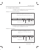
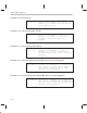

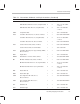
Table Of Contents
- Read This First
- Contents
- Figures
- Tables
- Examples
- Cautions
- Introduction
- Architectural Overview
- Central Processing Unit
- Memory and I/O Spaces
- Program Control
- Addressing Modes
- Assembly Language Instructions
- Instruction Set Summary
- How To Use the Instruction Descriptions
- Instruction Descriptions
- ABS
- ABS
- ADD
- ADD
- ADD
- ADD
- ADDC
- ADDC
- ADDS
- ADDS
- ADDT
- ADDT
- ADRK
- AND
- AND
- AND
- APAC
- APAC
- B
- BACC
- BANZ
- BANZ
- BCND
- BCND
- BIT
- BIT
- BITT
- BITT
- BLDD
- BLDD
- BLDD
- BLDD
- BLDD
- BLPD
- BLPD
- BLPD
- BLPD
- CALA
- CALL
- CC
- CC
- CLRC
- CLRC
- CMPL
- CMPR
- DMOV
- DMOV
- IDLE
- IN
- IN
- INTR
- LACC
- LACC
- LACC
- LACL
- LACL
- LACL
- LACT
- LACT
- LAR
- LAR
- LAR
- LDP
- LDP
- LPH
- LPH
- LST
- LST
- LST
- LST
- LT
- LT
- LTA
- LTA
- LTD
- LTD
- LTD
- LTP
- LTP
- LTS
- LTS
- MAC
- MAC
- MAC
- MAC
- MACD
- MACD
- MACD
- MACD
- MACD
- MAR
- MAR
- MPY
- MPY
- MPY
- MPYA
- MPYA
- MPYS
- MPYS
- MPYU
- MPYU
- NEG
- NEG
- NMI
- NOP
- NORM
- NORM
- NORM
- OR
- OR
- OR
- OUT
- OUT
- PAC
- POP
- POP
- POPD
- POPD
- PSHD
- PSHD
- PUSH
- RET
- RETC
- ROL
- ROR
- RPT
- RPT
- SACH
- SACH
- SACL
- SACL
- SAR
- SAR
- SBRK
- SETC
- SETC
- SFL
- SFR
- SFR
- SPAC
- SPH
- SPH
- SPL
- SPL
- SPLK
- SPLK
- SPM
- SQRA
- SQRA
- SQRS
- SQRS
- SST
- SST
- SUB
- SUB
- SUB
- SUB
- SUBB
- SUBB
- SUBC
- SUBC
- SUBS
- SUBS
- SUBT
- SUBT
- TBLR
- TBLR
- TBLR
- TBLW
- TBLW
- TBLW
- TRAP
- XOR
- XOR
- XOR
- ZALR
- ZALR
- On-Chip Peripherals
- Synchronous Serial Port
- Asynchronous Serial Port
- TMS320C209
- Register Summary
- TMS320C1x/C2x/C2xx/C5x Instruction Set Comparison
- Program Examples
- Submitting ROM Codes to TI
- Design Considerations for Using XDS510 Emulator
- E.1 Designing Your Target System’s Emulator Connector (14-Pin Header)
- E.2 Bus Protocol
- E.3 Emulator Cable Pod
- E.4 Emulator Cable Pod Signal Timing
- E.5 Emulation Timing Calculations
- E.6 Connections Between the Emulator and the Target System
- E.7 Physical Dimensions for the 14-Pin Emulator Connector
- E.8 Emulation Design Considerations
- Glossary
- Index

Instruction Set Summary
7-4
ZLVC ZLVC Two 4-bit fields — each representing the following conditions:
ACC = 0 Z
ACC < 0 L
Overflow V
Carry C
A conditional instruction contains two of these 4-bit fields. The
4-LSB field of the instruction is a mask field. A 1 in the corre-
sponding mask bit indicates that condition is being tested. For
example, to test for ACC ≥ 0, the Z and L fields are set, and
the V and C fields are not set. The Z field is set to test the condi-
tion ACC = 0, and the L field is reset to test the condition
ACC ≥ 0.The second 4-bit field (bits 4 – 7) indicates the state
of the conditions to test. The conditions possible with these
eight bits are shown in the descriptions for the BCND, CC, and
RETC instructions.
+ 1 word The second word of a two-word opcode. This second word
contains a 16-bit constant. Depending on the instruction, this
constant is a long immediate value, a program memory ad-
dress, or an address for an I/O port or an I/O-mapped register.
Table 7–1. Accumulator, Arithmetic, and Logic Instructions
Mnemonic Description Words Cycles Opcode
ABS Absolute value of ACC 1 1 1011 1110 0000 0000
ADD Add to ACC with shift of 0 to 15, direct or indirect 1 1 0010 SHFT IAAA AAAA
Add to ACC with shift 0 to 15, long immediate 2 2 1011 1111 1001 SHFT
+ 1 word
Add to ACC with shift of 16, direct or indirect 1 1 0110 0001 IAAA AAAA
Add to ACC, short immediate 1 1 1011 1000 IIII IIII
ADDC Add to ACC with carry, direct or indirect 1 1 0110 0000 IAAA AAAA
ADDS Add to low ACC with sign-extension suppressed,
direct or indirect
1 1 0110 0010 IAAA AAAA
ADDT
Add to ACC with shift (0 to 15) specified by TREG,
direct or indirect
1 1 0110 0011 IAAA AAAA