
User manual
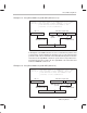
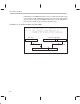

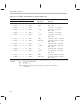
Table Of Contents
- Read This First
- Contents
- Figures
- Tables
- Examples
- Cautions
- Introduction
- Architectural Overview
- Central Processing Unit
- Memory and I/O Spaces
- Program Control
- Addressing Modes
- Assembly Language Instructions
- Instruction Set Summary
- How To Use the Instruction Descriptions
- Instruction Descriptions
- ABS
- ABS
- ADD
- ADD
- ADD
- ADD
- ADDC
- ADDC
- ADDS
- ADDS
- ADDT
- ADDT
- ADRK
- AND
- AND
- AND
- APAC
- APAC
- B
- BACC
- BANZ
- BANZ
- BCND
- BCND
- BIT
- BIT
- BITT
- BITT
- BLDD
- BLDD
- BLDD
- BLDD
- BLDD
- BLPD
- BLPD
- BLPD
- BLPD
- CALA
- CALL
- CC
- CC
- CLRC
- CLRC
- CMPL
- CMPR
- DMOV
- DMOV
- IDLE
- IN
- IN
- INTR
- LACC
- LACC
- LACC
- LACL
- LACL
- LACL
- LACT
- LACT
- LAR
- LAR
- LAR
- LDP
- LDP
- LPH
- LPH
- LST
- LST
- LST
- LST
- LT
- LT
- LTA
- LTA
- LTD
- LTD
- LTD
- LTP
- LTP
- LTS
- LTS
- MAC
- MAC
- MAC
- MAC
- MACD
- MACD
- MACD
- MACD
- MACD
- MAR
- MAR
- MPY
- MPY
- MPY
- MPYA
- MPYA
- MPYS
- MPYS
- MPYU
- MPYU
- NEG
- NEG
- NMI
- NOP
- NORM
- NORM
- NORM
- OR
- OR
- OR
- OUT
- OUT
- PAC
- POP
- POP
- POPD
- POPD
- PSHD
- PSHD
- PUSH
- RET
- RETC
- ROL
- ROR
- RPT
- RPT
- SACH
- SACH
- SACL
- SACL
- SAR
- SAR
- SBRK
- SETC
- SETC
- SFL
- SFR
- SFR
- SPAC
- SPH
- SPH
- SPL
- SPL
- SPLK
- SPLK
- SPM
- SQRA
- SQRA
- SQRS
- SQRS
- SST
- SST
- SUB
- SUB
- SUB
- SUB
- SUBB
- SUBB
- SUBC
- SUBC
- SUBS
- SUBS
- SUBT
- SUBT
- TBLR
- TBLR
- TBLR
- TBLW
- TBLW
- TBLW
- TRAP
- XOR
- XOR
- XOR
- ZALR
- ZALR
- On-Chip Peripherals
- Synchronous Serial Port
- Asynchronous Serial Port
- TMS320C209
- Register Summary
- TMS320C1x/C2x/C2xx/C5x Instruction Set Comparison
- Program Examples
- Submitting ROM Codes to TI
- Design Considerations for Using XDS510 Emulator
- E.1 Designing Your Target System’s Emulator Connector (14-Pin Header)
- E.2 Bus Protocol
- E.3 Emulator Cable Pod
- E.4 Emulator Cable Pod Signal Timing
- E.5 Emulation Timing Calculations
- E.6 Connections Between the Emulator and the Target System
- E.7 Physical Dimensions for the 14-Pin Emulator Connector
- E.8 Emulation Design Considerations
- Glossary
- Index
Direct Addressing Mode
6-7
Addressing Modes
Example 6–3. Using Direct Addressing with ADD (Shift of 0 to 15)
LDP #4 ;Set data page to 4 (addresses 0200h–027Fh).
ADD 9h,5 ;The contents of data address 0209h are
;left–shifted 5 bits and added to the
;contents of the accumulator.
7 LSBs from IR
16-bit data address 0209h
All 9 bits from DP
DP = 4 Instruction register (IR)
0 0 1 0
0 0 0 1 0 0 1
0 0 0 0 0 0 1 0 0 0
0 0 1 0
ADD
opcode
Shift of 5
0 0 0 0 0 0 1 0 0
0 0 0 1 0 0 1
9h
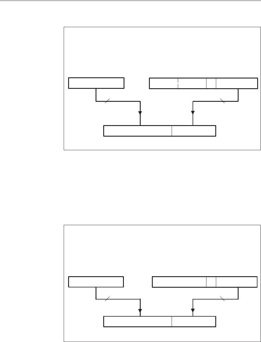
In Example 6–4, the ADD instruction references a data memory address that
is generated as shown following the program code. For any instruction that
performs a shift of 16, the shift value is not embedded directly in the instruction
word; instead, all eight MSBs contain an opcode that not only indicates the
instruction type but also a shift of 16. The eight MSBs of the instruction word
indicate an ADD with a shift of 16.
Example 6–4. Using Direct Addressing with ADD (Shift of 16)
LDP #5 ;Set data page to 5 (addresses 0280h–02FFh).
ADD 9h,16 ;The contents of data address 0289h are
;left–shifted 16 bits and added to the
;contents of the accumulator.
7 LSBs from IR
16-bit data address 0289h
All 9 bits from DP
DP = 5 Instruction register (IR)
0 0 0 1 0 0 10 0 0 0 0 0 1 0 1 0
ADD with shift of 16
opcode
0 0 0 0 0 0 1 0 1
0 0 0 1 0 0 1
9h
0 1 1 0 0 0 0 1