
User manual
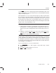

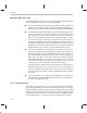
Table Of Contents
- Read This First
- Contents
- Figures
- Tables
- Examples
- Cautions
- Introduction
- Architectural Overview
- Central Processing Unit
- Memory and I/O Spaces
- Program Control
- Addressing Modes
- Assembly Language Instructions
- Instruction Set Summary
- How To Use the Instruction Descriptions
- Instruction Descriptions
- ABS
- ABS
- ADD
- ADD
- ADD
- ADD
- ADDC
- ADDC
- ADDS
- ADDS
- ADDT
- ADDT
- ADRK
- AND
- AND
- AND
- APAC
- APAC
- B
- BACC
- BANZ
- BANZ
- BCND
- BCND
- BIT
- BIT
- BITT
- BITT
- BLDD
- BLDD
- BLDD
- BLDD
- BLDD
- BLPD
- BLPD
- BLPD
- BLPD
- CALA
- CALL
- CC
- CC
- CLRC
- CLRC
- CMPL
- CMPR
- DMOV
- DMOV
- IDLE
- IN
- IN
- INTR
- LACC
- LACC
- LACC
- LACL
- LACL
- LACL
- LACT
- LACT
- LAR
- LAR
- LAR
- LDP
- LDP
- LPH
- LPH
- LST
- LST
- LST
- LST
- LT
- LT
- LTA
- LTA
- LTD
- LTD
- LTD
- LTP
- LTP
- LTS
- LTS
- MAC
- MAC
- MAC
- MAC
- MACD
- MACD
- MACD
- MACD
- MACD
- MAR
- MAR
- MPY
- MPY
- MPY
- MPYA
- MPYA
- MPYS
- MPYS
- MPYU
- MPYU
- NEG
- NEG
- NMI
- NOP
- NORM
- NORM
- NORM
- OR
- OR
- OR
- OUT
- OUT
- PAC
- POP
- POP
- POPD
- POPD
- PSHD
- PSHD
- PUSH
- RET
- RETC
- ROL
- ROR
- RPT
- RPT
- SACH
- SACH
- SACL
- SACL
- SAR
- SAR
- SBRK
- SETC
- SETC
- SFL
- SFR
- SFR
- SPAC
- SPH
- SPH
- SPL
- SPL
- SPLK
- SPLK
- SPM
- SQRA
- SQRA
- SQRS
- SQRS
- SST
- SST
- SUB
- SUB
- SUB
- SUB
- SUBB
- SUBB
- SUBC
- SUBC
- SUBS
- SUBS
- SUBT
- SUBT
- TBLR
- TBLR
- TBLR
- TBLW
- TBLW
- TBLW
- TRAP
- XOR
- XOR
- XOR
- ZALR
- ZALR
- On-Chip Peripherals
- Synchronous Serial Port
- Asynchronous Serial Port
- TMS320C209
- Register Summary
- TMS320C1x/C2x/C2xx/C5x Instruction Set Comparison
- Program Examples
- Submitting ROM Codes to TI
- Design Considerations for Using XDS510 Emulator
- E.1 Designing Your Target System’s Emulator Connector (14-Pin Header)
- E.2 Bus Protocol
- E.3 Emulator Cable Pod
- E.4 Emulator Cable Pod Signal Timing
- E.5 Emulation Timing Calculations
- E.6 Connections Between the Emulator and the Target System
- E.7 Physical Dimensions for the 14-Pin Emulator Connector
- E.8 Emulation Design Considerations
- Glossary
- Index

Interrupts
5-28
Note:
The INTR instruction does not affect IFR flags. When you use the INTR
instruction to initiate an interrupt that has an associated flag bit in the IFR,
the instruction neither sets nor clears the flag bit. No software write operation
can set the IFR flag bits; only the appropriate hardware requests can. If a
hardware request has set the flag for an interrupt and then the INTR instruc-
tion is used to initiate that interrupt, the INTR instruction will not clear the flag.
NMI. This instruction forces a branch to interrupt vector location 24h, the
same location used for the nonmaskable hardware interrupt NMI
. Thus,
you can either initiate NMI
by driving the NMI pin low or by executing an
NMI instruction. When the NMI instruction is executed, INTM is set to 1 to
disable maskable interrupts.
TRAP. This instruction forces the CPU to branch to interrupt vector loca-
tion 22h. The TRAP instruction does
not
disable maskable interrupts
(INTM is not set to 1); thus when the CPU branches to the interrupt service
routine, that routine can be interrupted by the maskable hardware inter-
rupts (in addition to RS
and NMI).
If the INTM bit is set to 1 during the acknowledgement process, all hardware-
initiated maskable interrupts are disabled and, thus, cannot interfere with the
interrupt service routine.
To determine which vector address has been assigned to each of the interrupts
on a specific ’C2xx device, see subsection 5.6.2 (on page 5-16). Interrupt vec-
tor locations are spaced apart by two addresses so that a 2-word branch
instruction can be accommodated in each location.
Figure 5–10 summarizes how nonmaskable interrupts are handled by the
CPU.