
User manual
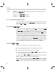
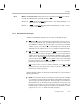

Table Of Contents
- Read This First
- Contents
- Figures
- Tables
- Examples
- Cautions
- Introduction
- Architectural Overview
- Central Processing Unit
- Memory and I/O Spaces
- Program Control
- Addressing Modes
- Assembly Language Instructions
- Instruction Set Summary
- How To Use the Instruction Descriptions
- Instruction Descriptions
- ABS
- ABS
- ADD
- ADD
- ADD
- ADD
- ADDC
- ADDC
- ADDS
- ADDS
- ADDT
- ADDT
- ADRK
- AND
- AND
- AND
- APAC
- APAC
- B
- BACC
- BANZ
- BANZ
- BCND
- BCND
- BIT
- BIT
- BITT
- BITT
- BLDD
- BLDD
- BLDD
- BLDD
- BLDD
- BLPD
- BLPD
- BLPD
- BLPD
- CALA
- CALL
- CC
- CC
- CLRC
- CLRC
- CMPL
- CMPR
- DMOV
- DMOV
- IDLE
- IN
- IN
- INTR
- LACC
- LACC
- LACC
- LACL
- LACL
- LACL
- LACT
- LACT
- LAR
- LAR
- LAR
- LDP
- LDP
- LPH
- LPH
- LST
- LST
- LST
- LST
- LT
- LT
- LTA
- LTA
- LTD
- LTD
- LTD
- LTP
- LTP
- LTS
- LTS
- MAC
- MAC
- MAC
- MAC
- MACD
- MACD
- MACD
- MACD
- MACD
- MAR
- MAR
- MPY
- MPY
- MPY
- MPYA
- MPYA
- MPYS
- MPYS
- MPYU
- MPYU
- NEG
- NEG
- NMI
- NOP
- NORM
- NORM
- NORM
- OR
- OR
- OR
- OUT
- OUT
- PAC
- POP
- POP
- POPD
- POPD
- PSHD
- PSHD
- PUSH
- RET
- RETC
- ROL
- ROR
- RPT
- RPT
- SACH
- SACH
- SACL
- SACL
- SAR
- SAR
- SBRK
- SETC
- SETC
- SFL
- SFR
- SFR
- SPAC
- SPH
- SPH
- SPL
- SPL
- SPLK
- SPLK
- SPM
- SQRA
- SQRA
- SQRS
- SQRS
- SST
- SST
- SUB
- SUB
- SUB
- SUB
- SUBB
- SUBB
- SUBC
- SUBC
- SUBS
- SUBS
- SUBT
- SUBT
- TBLR
- TBLR
- TBLR
- TBLW
- TBLW
- TBLW
- TRAP
- XOR
- XOR
- XOR
- ZALR
- ZALR
- On-Chip Peripherals
- Synchronous Serial Port
- Asynchronous Serial Port
- TMS320C209
- Register Summary
- TMS320C1x/C2x/C2xx/C5x Instruction Set Comparison
- Program Examples
- Submitting ROM Codes to TI
- Design Considerations for Using XDS510 Emulator
- E.1 Designing Your Target System’s Emulator Connector (14-Pin Header)
- E.2 Bus Protocol
- E.3 Emulator Cable Pod
- E.4 Emulator Cable Pod Signal Timing
- E.5 Emulation Timing Calculations
- E.6 Connections Between the Emulator and the Target System
- E.7 Physical Dimensions for the 14-Pin Emulator Connector
- E.8 Emulation Design Considerations
- Glossary
- Index
Interrupts
5-26
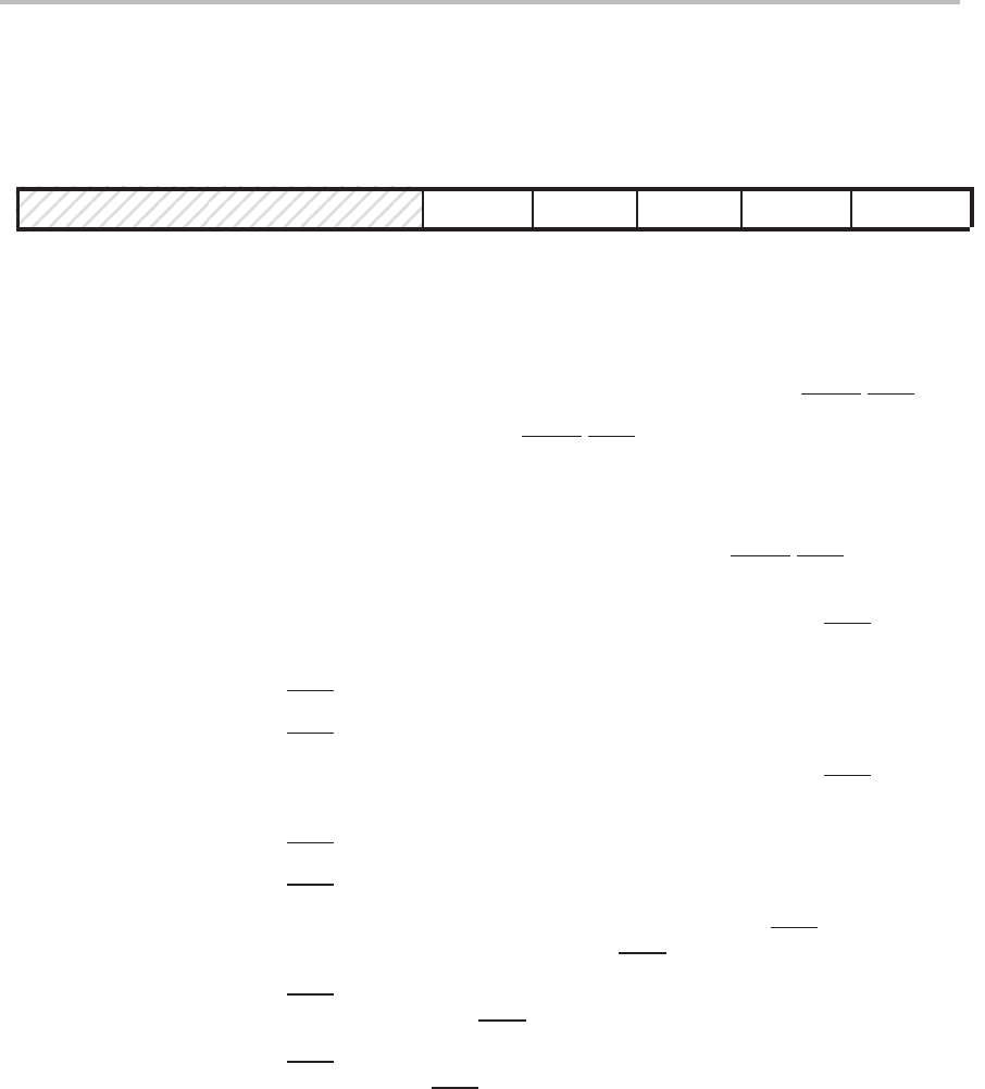
Figure 5–9 shows the ICR, and bit descriptions follow the figure.
Figure 5–9. ’C2xx Interrupt Control Register (ICR) — I/O-Space Address FFECh
15 5 4 3 2 1 0
Reserved MODE FINT3 FINT2 MINT3 MINT2
0 R/W–0 R/W1C–0 R/W1C–0 R/W–0 R/W–0
Note: 0 = Always read as zeros; R = Read access; W = Write access; W1C = Write 1 to this bit to clear it to 0;
value following dash (–) is value after reset.
Bits 15–5 Reserved. Bits 15–5 are reserved and are always read as 0s.
Bit 4 MODE — Pin mode. Bit 4 selects one of two possible modes for the HOLD
/INT1 pin.
MODE = 0
Double-edge mode.
The HOLD/INT1 pin is both negative- and positive-
edge sensitive. A falling edge or a rising edge triggers an interrupt re-
quest. This mode is necessary for proper implementation of a HOLD op-
eration.
MODE = 1
Single-edge mode.
A falling edge (only) on the HOLD/INT1 pin triggers
an interrupt request.
Bit 3 FINT3 — Interrupt 3 flag. If MINT3 = 1, an interrupt request on the INT3
pin sets
FINT3 and bit 1 of the IFR (INT2/INT3).
FINT3 = 0 INT3
is not pending.
FINT3 = 1 INT3
is pending.
Bit 2 FINT2 — Interrupt 2 flag. If MINT2 = 1, an interrupt request on the INT2
pin sets
FINT2 and bit 1 of the IFR (INT2/INT3).
INT2 = 0 INT2
is not pending.
INT2 = 1 INT2
is pending.
Bit 1 MINT3 — Interrupt 3 mask. This bit masks the external interrupt INT3
or, in conjunc-
tion with the INT2/INT3 bit of the IMR, unmasks INT3
.
MINT3 = 0 INT3
is masked. Neither FINT3 nor bit 1 of the IFR (INT2/INT3) is set
by a request on the INT3
pin.
MINT3 = 1 INT3
is unmasked. Flag bits FINT3 and INT2/INT3 are both set by a
request on the INT3
pin.