
Datasheet
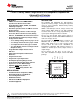


bq24707
bq24707A
www.ti.com
SLUSA78B –JULY 2010– REVISED MARCH 2011
ELECTRICAL CHARACTERISTICS (continued)
4.5 V ≤ V
(VCC)
≤ 24 V, 0°C ≤ T
J
≤ 125°C, typical values are at T
A
= 25°C, with respect to GND (unless otherwise noted)
PARAMETER TEST CONDITIONS MIN TYP MAX UNIT
SMBus TIMING CHARACTERISTICS
t
R
SCLK/SDATA rise time 1 μs
t
F
SCLK/SDATA fall time 300 ns
t
W(H)
SCLK pulse width high 4 50 μs
t
W(L)
SCLK pulse width low 4.7 μs
t
SU(STA)
Setup time for START condition 4.7 μs
START condition hold time after which first clock
t
H(STA)
4 μs
pulse is generated
t
SU(DAT)
Data setup time 250 ns
t
H(DAT)
Data hold time 300 ns
t
SU(STOP)
Setup time for STOP condition 4 µs
t
(BUF)
Bus free time between START and STOP condition 4.7 μs
F
S(CL)
Clock frequency 10 100 kHz
HOST COMMUNICATION FAILURE
t
timeout
SMBus bus release timeout
(3)
25 35 ms
t
BOOT
Deglitch for watchdog reset signal 10 ms
Watchdog timeout period, ChargeOption()
t
WDI
35 44 53 s
bit [14:13] = 01
(4)
Watchdog timeout period, ChargeOption()
t
WDI
70 88 105 s
bit [14:13] = 10
(4)
Watchdog timeout period, ChargeOption()
t
WDI
140 175 210 s
bit [14:13] = 11
(4)
(default)
(3) Devices participating in a transfer timeout when any clock low exceeds the 25ms minimum timeout period. Devices that have detected a
timeout condition must reset the communication no later than the 35ms maximum timeout period. Both a master and a slave must
adhere to the maximum value specified as it incorporates the cumulative stretch limit for both a master (10ms) and a slave (25ms).
(4) User can adjust threshold via SMBus ChargeOption() REG0x12.
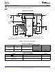
Figure 2. SMBus Communication Timing Waveforms
© 2010–2011, Texas Instruments Incorporated Submit Documentation Feedback 7
Product Folder Link(s): bq24707 bq24707A