
Datasheet


Table Of Contents
- FEATURES
- DESCRIPTION
- PIN CONNECTIONS
- ABSOLUTE MAXIMUM RATINGS
- DC ELECTRICAL CHARACTERISTICS
- VFC CHARACTERISTICS
- REG CHARACTERISTICS
- SMBus AC SPECIFICATIONS
- HDQ16 AC SPECIFICATIONS
- FUNCTIONAL DESCRIPTION
- General Operation
- Measurements
- Current
- Temperature
- GAS GAUGE OPERATION
- MAIN GAS GAUGE REGISTERS
- Self-Discharge
- Light Discharge or Suspend Current Compensation
- Midrange Capacity Corrections
- Charge Control
- Display Port
- Secondary Protection for Li-ion
- Low-Power Storage Mode
- Device Reset
- COMMUNICATION
- SMBus
- SMBus Protocol
- SMBus Packet Error Checking
- PEC Protocol
- PEC Calculation
- PEC Enable in Master Mode
- SMBus On and Off State
- HDQ16
- Command Codes
- ManufacturerAccess() (0x00); [0x00–0x01]
- RemainingCapacityAlarm() (0x01); [0x01]
- RemainingTimeAlarm() (0x02); [0x02]
- BatteryMode() (0x03); [0x03]
- AtRate() (0x04); [0x04]
- AtRateTimeToFull() (0x05);[0x05]
- AtRateTimeToEmpty() (0x06); [0x06]
- AtRateOK() (0x07); [0x07]
- Temperature() (0x08); [0x08]
- Voltage() (0x09); [0x09]
- Current() (0x0a); [0x0a]
- AverageCurrent() (0x0b); [0x0b]
- MaxError() (0x0c); [0x0c]
- RelativeStateOfCharge() (0x0d); [0x0d]
- AbsoluteStateOfCharge()(0x0e); [0x0e]
- RemainingCapacity() (0x0f); [0x0f]
- FullChargeCapacity() (0x10); [0x10]
- RunTimeToEmpty() (0x11); [0x11]
- AverageTimeToEmpty() (0x12); [0x12]
- AverageTimeToFull() (0x13); [0x13]
- ChargingCurrent() (0x14); [0x14]
- ChargingVoltage() (0x15); [0x15]
- BatteryStatus()(0x16); [0x16]
- CycleCount()(0x17); [0x17]
- DesignCapacity() (0x18); [0x18]
- DesignVoltage() (0x19); [0x19]
- SpecificationInfo() (0x1a); [0x1a]
- ManufactureDate() (0x1b); [0x1b]
- SerialNumber() (0x1c); [0x1c]
- ManufacturerName() (0x20); [0x20–0x2a]
- DeviceName() (0x21); [0x28–0x2b]
- DeviceChemistry() (0x22); [0x30–0x32]
- ManufacturerData() (0x23); [0x38–0x3a]
- Pack Status and Pack Configuration (0x2f); [0x2f]
- OCE
- EDV2
- EINT
- VDQ
- COK
- DOK
- CVOV
- CVUV
- VCELL4–VCELL1 (0x3c–0x3f); [0x3c–0x3f]
- EEPROM
- EEPROM Programming
- Fundamental Parameters
- Cell Characteristics
- Charge Limits and Termination Techniques
- Overvoltage
- Charging Current
- Charge Suspension
- FULLY_CHARGED Bit Clear Threshold
- Fast Charge Termination Percentage
- Cycle Count Threshold
- ΔT/Δt Rate Programming
- ΔT/Δt Holdoff Timer Programming
- Current Taper Termination Characteristics
- PACK OPTIONS
- DMODE
- SEAL
- CSYNC
- CEDV
- VCOR
- CHEM
- LCC0 and LCC1
- Remaining Time and Capacity Alarms
- Secondary Protection Limits for Li-Ion
- Miscellaneous Options
- NE1
- SOT
- HIT
- Cycle Count Initialization
- Control Modes
- NDF
- HPE
- CPE
- LED
- SC
- SM
- MEASUREMENT CALIBRATION
- CONSTANTS AND STRING DATA
- REVISION HISTORY
bq2060A
SLUS500D –OCTOBER 2001– REVISED OCTOBER 2011
www.ti.com
This integrated circuit can be damaged by ESD. Texas Instruments recommends that all integrated circuits be handled with
appropriate precautions. Failure to observe proper handling and installation procedures can cause damage.
ESD damage can range from subtle performance degradation to complete device failure. Precision integrated circuits may be more
susceptible to damage because very small parametric changes could cause the device not to meet its published specifications.
Pin Descriptions
PIN
DESCRIPTION
NAME NUMBER
HDQ16 1 Serial communication input/output. Open-drain bidirectional communications port
Serial memory clock. Output to clock the data transfer between the bq2060A and the external nonvolatile
ESCL 2
configuration memory
Serial memory data and address. Bidirectional pin used to transfer address and data to and from the bq2060A
ESDA 3
and the external nonvolatile configuration memory.
Register backup input. Input that provides backup potential to the bq2060A registers during periods of low
RBI 4
operating voltage. RBI accepts a storage capacitor or a battery input.
REG 5 Regulator output. Output to control an n-JFET for VCC regulation to the bq2060A from the battery potential
V
OUT
(1)
6 EEPROM supply output. Output that supplies power to the external EEPROM configuration memory
V
CC
(1)
7 Supply voltage input
V
SS
8 Ground
DISP 9 Display control input. Input that controls the LED drivers LED
1
–LED
5
LED
1
–LED
5
10–14 LED display segment outputs. Outputs that each may drive an external LED
DFC 15 Discharge FET control. Output to control the discharge FET in the Li-ion pack protection circuitry
CFC 16 Charge FET control output. Output to control the charge FET in the Li-ion pack protection circuitry
Cell voltage divider control output. Output control for external FETs to connect the cells to the external voltage
CVON 17
dividers during cell voltage measurements
Thermistor bias control. Output control for external FETs to connect the thermistor bias resistor during a
THON 18
temperature measurement
TS 19 Thermistor voltage input. Input connection for a thermistor to monitor temperature
SRC 20 Current sense input. Input to monitor instantaneous current
Charge-flow sense resistor inputs. Input connections for a small value sense resistor to monitor the battery
SR
1
– SR
2
21–22
charge and discharge current flow
VCELL
1
–VC
23–26 Single-cell voltage inputs. Inputs that monitor the series element cell voltages
ELL
4
SMBD 27 SMBus data. Open-drain bidirectional pin used to transfer address and data to and from the bq2060A
SMBC 28 SMBus clock. Open-drain bidirectional pin used to clock the data transfer to and from the bq2060A
(1) CAUTION: Recent changes to some EEPROM ICs have made the timing of the V
OUT
pin unreliable. It is strongly recommended that the
EEPROM is powered from the V
CC
pin (pin 7). Also, it is acceptable to short pins 6 and 7, if needed.
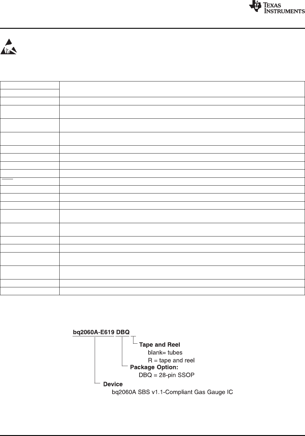
ORDERING INFORMATION
(1) For the most current package and ordering information, see the Package Option Addendum at the end of this
document, or see the TI Web site at www.ti.com.
2 Submit Documentation Feedback Copyright © 2001–2011, Texas Instruments Incorporated
Product Folder Link(s): bq2060A