
User manual

+
+
+
Vin-12v
Boost
V-boost1
V-boost2
V-boost6
1A
1B
3B
I-Led6
I-Led2 I-Led1
F28027
3V3
Comms
CPU
32 bit
DSP core
60 MHz
I C
SPI
UART
2
ADC
12 bit
4.6 MSPS
I-Led1
I-Led2
I-Led8
V-boost1
V-boost6
V-sepic1
V-sepic2
1A / 1B
2A / 2B
3A / 3B
4A / 4B
PWM1
(HR)
PWM2
(HR)
PWM3
(HR)
PWM4
(HR)
Vref
www.ti.com
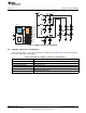
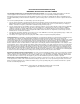
Hardware Resource Mapping
Figure 8. LED BoosterPack Circuit Diagram
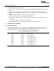
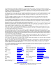
5.2 Jumpers, Connectors, and Switches
Table 3 lists the jumpers, connectors, and switches available on the board. Figure 9 shows the location of
these items with help of a board image.
Table 3. Description of Jumpers, Connectors, and Switches
J1 Barrel Jack for main power connection (6 V-48 V)
J2 Jumper to connect BoosterPack 3.3 V to LaunchPad Headers
J8 Jumper to connect BoosterPack 5 V to LaunchPad Headers
J3, J9 and J4, J10 and J11 LaunchPadXL Socket
J6 and J7 Capacitive Touch BoosterPack Headers
S1 MSP430 Serial Disconnect Switch
J5 MSP430 Programming Header
13
SPRUHH9–July 2012 C2000 LED BoosterPack
Submit Documentation Feedback
Copyright © 2012, Texas Instruments Incorporated