
User manual


0 Ω
R27
0 Ω
R24 IN_N
IN_P
0.01 Fµ
C12
TP13
TP14
DET_N
DET_P
1.00 kΩ
R28
VCM_SHIELD
TP8
VBG
TX_N
TX_P
TP17
TX_LED_N
TX_LED_P
TP30
AFE_PDNZ
AFE_PDNZ
TP22
AFE_RESETZ
ADC_RDY
STE
SIMO
SOMI
SCLK
PD_ALM
LED_ALM
DIAG_END
TP6
TP20
0.1 Fµ
C10
XIN_MSP
LED_DRV_SUP
RX_DIG_SUP
RX_DIG_SUP
TX_CTRL_SUP
BAV99W-7-F
75 V
1
3
2
D1
BAV99W-7-F
75 V
1
3
2
D2
RX_ANA_SUP
VCM_AFE
2.2 Fµ
C41
2.2 µF
C42
0.1 µF
C16
TP25
BAV99W-7-F
75 V
1
3
2
D3
BAV99W-7-F
75 V
1
3
2
D4
LED_DRV_SUP
1 Fµ
C15
0.1 µF
C9
RX_ANA_SUP
AFE_CLKOUT
TP7
TP12
R32 130 Ω
R36 130 Ω
R40 130 Ω
R22 130 Ω
R20 130 Ω
NellCor DS-100A PulseOx Connectors
0 Ω
Jumper
R44
0 Ω
Jumper
R48
R41 130 Ω
DB9-F
1
2
3
4
5
6
7
8
9
11
10
J2
DB9-F-TP
INM
1
INP
2
RX_ANA_GND
3
VCM
4
DNC
5
DNC
6
BG
7
VSS
8
RSVD
9
DNC
10
TX_CTRL_SUP
11
LED_DRV_GND
12
LED_DRV_GND
13
TXM
14
TXP
15
LED_DRV_GND
16
LED_DRV_SUP
17
LED_DRV_SUP
18
RX_DIG_GND
19
AFE_PDNZ
20
DIAG_END
21
LED_ALM
22
PD_ALM
23
SPI_CLK
24
SPI_SOMI
25
SPI_SIMO
26
SPI_STE
27
ADC_RDY
28
RESETZ
29
CLK_OUT
30
RX_DIG_SUP
31
RX_DIG_GND
32
RX_ANA_SUP
33
RX_OUTN
34
RX_OUTP
35
RX_ANA_GND
36
XOUT
37
XIN
38
RX_ANA_SUP
39
RX_ANA_GND
40
EP
41
AFE4400
U1
0 Ω
DNI
R15
0 Ω
R16
0 Ω
R17
TP11
R23 10 Ω
AFE44x0
18 pF
C7
18 pF
C6
1 2
8 MHz
Y1
TP23
10 kΩ
R98
The following signals need to be considered as two sets of
differential pairs and routed as adjacent signals within each pair.
1. TXM and TXP
2. INM and INP
INM and INP must be guarded with VCM_SHIELD signal.
Run the VCM_SHIELD signal to the DB9 connector and back to
the device.
www.ti.com
PCB Layouts and Schematics
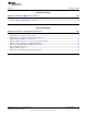
12.2 AFE44x0SPO2EVM Schematics
Figure 69 through Figure 72 show the EVM schematics (landscaped for readability).
Figure 69. AFE44x0SPO2EVM: AFE44x0 Schematic (1 of 4)
55
SLAU480C–January 2013–Revised May 2014 AFE4400 and AFE4490 Development Guide
Submit Documentation Feedback
Copyright © 2013–2014, Texas Instruments Incorporated