
Datasheet
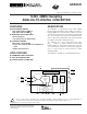

ADS5421
3
SBAS237E
www.ti.com
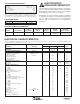
DIGITAL INPUTS
Clock Input Rising Edge of Convert Clock +0.5 +V
SD
V
PP
Logic Family (other than clock inputs) +3V/+5V Compatible CMOS
High Level Input Current
(5)
(V
IN
= 5V) 100 µA
Low Level Input Current (V
IN
= 0V) 10 µA
High Level Input Voltage +2.0 V
Low Level Input Voltage +1.0 V
Input Capacitance 5pF
DIGITAL OUTPUTS
(6)
Logic Family +3V/+5V Compatible CMOS
Logic Coding Straight Offset Binary
Low Output Voltage (I
OL
= 50µA to 0.5mA) VDRV = 3V +0.2 V
High Output Voltage (I
OH
= 50µA to 0.5mA) +2.5 V
Low Output Voltage (I
OL
= 50µA to 1.6mA) VDRV = 5V +0.2 V
High Output Voltage (I
OH
= 50µA to 1.6mA) +2.5 V
3-State Enable Time OE = LOW 20 40 ns
3-State Disable Time OE = HIGH 2 10 ns
Output Capacitance 5pF
ACCURACY
Zero Error (Referred to –FS) at +25°C ±0.5 ±1.0 %FS
Zero Error Drift (Referred to –FS) 15 ppm/°C
Gain Error
(7)
at +25°C ±0.2 ±1.0 %FS
Gain Error Drift
(7)
35 ppm/°C
Power-Supply Rejection of Gain ∆V
S
= ±5% 68 dB
Internal REF Tolerance (V
REFT
, V
REFB
) Deviation from Ideal ±10 ±50 mV
External REF Voltage Range (V
REFT
– V
REFB
) 1.4 2 2.025 V
Reference Input Resistance 1.0 kΩ
POWER-SUPPLY REQUIREMENTS
Supply Voltage: +V
SA
, +V
SD
Operating, f
IN
= 10MHz +4.75 +5.0 +5.25 V
Supply Current: +I
S
Operating, f
IN
= 10MHz 170 mA
Output Driver Supply Current (VDRV) 12 mA
Power Dissipation: VDRV = 5V 900 mW
VDRV = 3V 850 925 mW
Power Down Operating 40 mW
Thermal Resistance,
θ
JA
LQFP-64 48 °C/W
NOTES: (1) Spurious-Free Dynamic Range refers to the magnitude of the largest harmonic. (2) dBFS means dB relative to Full-Scale. (3) 2-tone intermodulation
distortion is referred to the largest fundamental tone. This number will be 6dB higher if it is referred to the magnitude of the 2-tone fundamental envelope.
(4) Effective Number of Bits (ENOB) is defined by (SINAD – 1.76)/6.02. (5) A 50kΩ pull-down resistor is inserted internally. (6) Recommended maximum
capacitance loading, 15pF. (7) Includes internal reference.
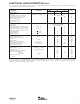
ELECTRICAL CHARACTERISTICS (Cont.)
T
A
= specified temperature range, typical at +25°C, +V
SA
= +V
SD
= +5V, differential input range = 1.5V to 3.5V each input (4V
PP
), sampling rate = 40MHz, internal
reference, VDRV = +3V, and –1dBFS, unless otherwise noted.
ADS5421Y
PARAMETER CONDITIONS MIN TYP MAX UNITS