
Datasheet
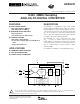

ADS5421
2
SBAS237E
www.ti.com
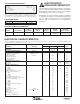
ELECTRICAL CHARACTERISTICS
T
A
= specified temperature range, typical at +25°C, +V
SA
= +V
SD
= +5V, differential input range = 1.5V to 3.5V each input (4V
PP
), sampling rate = 40MHz, internal
reference, VDRV = +3V, and –1dBFS, unless otherwise noted.
ADS5421Y
PARAMETER CONDITIONS MIN TYP MAX UNITS
RESOLUTION 14 Tested Bits
SPECIFIED TEMPERATURE RANGE Ambient Air –40 to +85 °C
ANALOG INPUT
Standard Differential Input Range Full-Scale = 4V
PP
1.5 3.5 V
Common-Mode Voltage 2.5 V
Optional Input Range Selectable 3V
PP
V
Analog Input Bias Current 1 µA
Analog Input Bandwidth 500 MHz
Input Capacitance 9pF
CONVERSION CHARACTERISTICS
Sample Rate 1M 40M Samples/sec
Data Latency 10 Clk Cyc
DYNAMIC CHARACTERISTICS
Differential Linearity Error (largest code error)
f = 1MHz ±0.5 LSB
f = 10MHz ±0.5 ±1.0 LSB
No Missing Codes Tested
Integral Nonlinearity Error, f = 1MHz ±2.5 LSB
Spurious-Free Dynamic Range
(1)
f = 1MHz 88 dBFS
(2)
f = 10MHz 78 85 dBFS
f = 30MHz 82 dBFS
2-Tone Intermodulation Distortion
(3)
f = 14.5MHz and 15.5MHz (–7dB each tone) –90 dBc
Signal-to-Noise Ratio (SNR)
f = 1MHz 76 dBFS
f = 10MHz 72 75 dBFS
f = 30MHz 75 dBFS
Signal-to-(Noise + Distortion) (SINAD)
f = 1MHz 75 dB
f = 10MHz 72 74 dB
f = 30MHz 74 dBFS
Effective Number of Bits
(4)
f = 1MHz 12.2 Bits
Output Noise IN and IN tied to CM 0.4 LSB rms
Aperture Delay Time 3ns
Aperture Jitter 1 ps rms
Over-Voltage Recovery Time 5ns
Full-Scale Step Acquisition Time 5ns
ELECTROSTATIC
DISCHARGE SENSITIVITY
This integrated circuit can be damaged by ESD. Texas Instru-
ments recommends that all integrated circuits be handled with
appropriate precautions. Failure to observe proper handling
and installation procedures can cause damage.
ESD damage can range from subtle performance degradation
to complete device failure. Precision integrated circuits may be
more susceptible to damage because very small parametric
changes could cause the device not to meet its published
specifications.
+V
SA
, +V
SD
, VDRV ............................................................................... +6V
Analog Input .......................................................... (–0.3V) to (+V
S
+ 0.3V)
Logic Input ............................................................ (–0.3V) to (+V
S
+ 0.3V)
Case Temperature ......................................................................... +100°C
Junction Temperature .................................................................... +150°C
Storage Temperature ..................................................................... +150°C
NOTE: (1) Stresses above these ratings may cause permanent damage.
Exposure to absolute maximum conditions for extended periods may degrade
device reliability. These are stress ratings only, and functional operation of the
device at these or any other conditions beyond those specified is not implied.
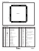
ABSOLUTE MAXIMUM RATINGS
(1)
SPECIFIED
PACKAGE TEMPERATURE PACKAGE ORDERING TRANSPORT
PRODUCT PACKAGE-LEAD DESIGNATOR RANGE MARKING NUMBER MEDIA, QUANTITY
ADS5421Y LQFP-64 PM –40°C to +85°C ADS5421Y ADS5421Y/T Tape and Reel, 250
" """"ADS5421Y/R Tape and Reel, 1500
PACKAGE/ORDERING INFORMATION
(1)
NOTE: (1) For the most current package and ordering information, see the Package Option Addendum at the end of this document, or see the TI website at
www.ti.com.
PRODUCT DESCRIPTION USER’S GUIDE
ADS5421EVM Populated Evaluation Board SBAU084
EVALUATION BOARD