
Datasheet


ADS5421
15
SBAS237E
www.ti.com
The clock inputs of the ADS5421 can be connected in a
number of ways. However, the best performance is obtained
when the clock input pins are driven differentially. Operating in
this mode, the clock inputs accommodate signal swings rang-
ing from 2.5V
PP
down to 0.5V
PP
differentially. This allows direct
interfacing of clock sources such as voltage-controlled crystal
oscillators (VCXO) to the ADS5421. The advantage here is the
elimination of external logic, usually necessary to convert the
clock signal into a suitable logic (TTL or CMOS) signal that
otherwise would create an additional source of jitter. In any
case, a very low-jitter clock is fundamental to preserving the
excellent AC performance of the ADS5421. The converter
itself is specified for a low jitter, characterizing the outstanding
capability of the internal clock and track-and-hold circuitry.
Generally, as the input frequency increases, the clock jitter
becomes more dominant for maintaining a good signal-to-
noise ratio. This is particularly critical in IF sampling applica-
tions where the sampling frequency is lower than input fre-
quency (undersampling). The following equation can be used
to calculate the achievable SNR for a given input frequency
and clock jitter (t
JA
in ps rms):
SNR 20 log
1
2 f t
10
IN JA
=
(
)
π
(2)
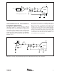
Depending on the nature of the clock source output imped-
ance, impedance matching might become necessary. For
this, a termination resistor, R
T
, can be installed (see Figure
12). To calculate the correct value for this resistor, consider
the impedance ratio of the selected transformer and the
differential clock input impedance of the ADS5421, which is
approximately 5.5kΩ.
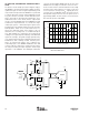
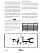
Shown in Figure 13 is one preferred method for clocking the
ADS5421. Here, the single-ended clock source can be either
a square wave or a sine wave. Using the high-speed differ-
ential translator SN65LVDS100 from Texas Instruments, a
low-jitter clock can be generated to drive the clock inputs of
the ADS5421 differentially.
MINIMUM SAMPLING RATE
The pipeline architecture of the ADS5421 uses a switched-
capacitor technique in its internal track-and-hold stages. With
each clock cycle, charges representing the captured signal
level are moved within the ADC pipeline core. The high
sampling speed necessitates the use of very small capacitor
values. In order to hold the droop errors low, the capacitors
require a minimum refresh rate. To maintain accuracy of the
acquired sample charge, the sampling clock on the ADS5421
must not drop below the specified minimum of 1MHz.
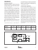
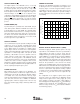
DATA OUTPUT FORMAT (BTC)
The ADS5421 makes two data output formats available,
either the Straight Offset Binary (SOB) code or the Binary
Two’s Complement (BTC) code. The selection of the output
coding is controlled through the BTC pin. Applying a logic
HIGH will enable the BTC coding, whereas a logic LOW will
enable the SOB code. The BTC output format is widely used
to interface to microprocessors, for example. The two code
structures are identical with the exception that the MSB is
inverted for the BTC format, as shown in Table II.
If the input signal exceeds the full-scale range, the data
outputs will exhibit the respective full-scale code depending
on the selected coding format.
ADS5421
CLK
CLK
R
T
(1)
50Ω
Square Wave
Or Sine Wave
Clock Input
100Ω
50Ω
+5V
0.01µF
0.01µF
0.01µF
0.01µF
Y
A
B
V
BB
Z
0.01µF
NOTE: (1) Additional termination resistor RT may be necessary depending on the source requirements
SN65LVDS100
FIGURE 13. Differential Clock Driver Using an LVDS Translator.
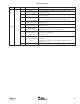
BINARY TWO’S
DIFFERENTIAL STRAIGHT OFFSET COMPLEMENT
INPUT BINARY (SOB) (BTC)
+FS – 1LSB 11 1111 1111 1111 01 1111 1111 1111
(IN = +3.5V, IN = +1.5V)
+1/2 FS 11 0000 0000 0000 01 0000 0000 0000
Bipolar Zero 10 0000 0000 0000 00 0000 0000 0000
(IN = IN = V
CM
)
–1/2 FS 01 0000 0000 0000 11 0000 0000 0000
–FS 00 0000 0000 0000 10 0000 0000 0000
(IN = +1.5V, IN = +3.5V)
TABLE II. Coding Table for Differential Input Configuration
and 4V
PP
Full-Scale Input Range.