
Datasheet


ADS5421
13
SBAS237E
www.ti.com
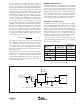
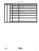
DESIRED FULL-SCALE
RANGE (FSR) CONNECT CONNECT VOLTAGE AT V
REF
VOLTAGE AT REFT VOLTAGE AT REFB
(DIFFERENTIAL) SEL1 (PIN 45) TO: SEL2 (PIN 44) TO: (PIN 46) (PIN 52) (PIN 50)
4V
PP
(+16dBm) GND GND +2.0V +3.5V +1.5V
3V
PP
(+13dBm) GND +V
SA
+1.5V +3.25V +1.75V
External Reference ——> +3.5V +3.2V to +3.5V +1.5V to +1.8V
TABLE I. Reference Pin Configurations and Corresponding Voltages on the Reference Pins.
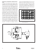
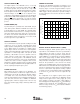
FIGURE 8. Internal Reference Circuit of the ADS5421 and Recommended Bypass Scheme.
Range Select
and
Gain Amplifier
Top
Reference
Driver
Bottom
Reference
Driver
+1V
DC
Bandgap
Reference
ADS5421
+
+
+
REFT
CM
REFB
2.2µF
2.2µF
2.2µF
0.1µF
0.1µF
0.1µF
0.1µF
0.1µF
REFBY
SEL1 SEL2
V
REF
500Ω
500Ω
45
61
46
44
52
51
50
REFERENCE
REFERENCE OPERATION
Integrated into the ADS5421 is a bandgap reference circuit,
including logic that provides a +1.5V or +2V reference
output by selecting the corresponding pin-strap configura-
tion. Table I lists an overview of the possible reference
options and pin configurations.
Figure 8 shows the basic model of the internal reference
circuit. The functional blocks are a 1V bandgap voltage
reference, a selectable gain amplifier, the drivers for the top
and bottom reference (REFT, REFB), and the resistive refer-
ence ladder. The ladder resistance measures approximately
1kΩ between the REFT and REFB pins. The ladder is split
into two equal segments establishing a common-mode volt-
age at the ladder midpoint, labeled CM. The ADS5421
requires solid bypassing for all reference pins to keep the
effects of clock feedthrough to a minimum and to achieve the
specified level of performance. Figure 8 shows the recom-
mended decoupling scheme. All 0.1µF capacitors must be
located as close to the pins as possible. In addition, pins
REFT, CM, and REFB must be decoupled with tantalum
surface-mount capacitors (2.2µF or 4.7µF).
When operating the ADS5421 with the internal reference, the
effective full-scale input span for each of the inputs, IN and
IN
, is determined by the voltage at the V
REF
pin, given to:
(1)
Input Span (differential, each input) = V
REF
= (REFT – REFB) in V
PP
The top and bottom reference outputs can be used to provide
up to 1mA of current (sink or source) to external circuits.
Degradation of the differential linearity (DNL) and, conse-
quently, the dynamic performance, of the ADS5421 may
occur if this limit is exceeded.
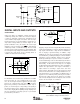
USING EXTERNAL REFERENCES
For even more design flexibility, the ADS5421 can be oper-
ated with external references. The utilization of an external
reference voltage may be considered for applications requir-
ing higher accuracy, improved temperature stability, or a
continuous adjustment of the converter full-scale range.
Especially in multichannel applications, the use of a common
external reference offers the benefit of improving the gain
matching between converters. Selection between internal or
external reference operation is controlled through the V
REF
pin. The internal reference will become disabled if the voltage
applied to the V
REF
pin exceeds +3.5V
DC
. Once selected, the
ADS5421 requires two reference voltages: a top reference
voltage applied to the REFT pin and a bottom reference
voltage applied to the REFB pin (see Table I). The full-scale
range is determined by FSR = 2 x (V
REFT
– V
REFB
). It is
recommended to maintain the common-mode voltage at
+2.5V. As illustrated in Figure 9, a micropower reference
(REF1004) and a dual, single-supply amplifier (OPA2234)
can be used to generate a precision external reference. Note
that the function of the range select pins, SEL1 and SEL2,
are disabled while the converter is operating in external
reference mode.