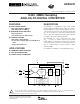
ADS5421 ADS 542 1 SBAS237E – DECEMBER 2001 – REVISED JUNE 2005 14-Bit, 40MHz Sampling ANALOG-TO-DIGITAL CONVERTER FEATURES DESCRIPTION ● HIGH DYNAMIC RANGE: High SFDR: 83dB at 10MHz fIN High SNR: 75dB at 10MHz fIN ● ON-BOARD TRACK-AND-HOLD: Differential Inputs Selectable Full-Scale Input Range ● FLEXIBLE CLOCKING: Differential or Single-Ended Accepts Sine or Square Wave Clocking Down to 0.
ELECTROSTATIC DISCHARGE SENSITIVITY ABSOLUTE MAXIMUM RATINGS(1) +VSA, +VSD, VDRV ............................................................................... +6V Analog Input .......................................................... (–0.3V) to (+VS + 0.3V) Logic Input ............................................................ (–0.3V) to (+VS + 0.3V) Case Temperature ......................................................................... +100°C Junction Temperature ..................................
ELECTRICAL CHARACTERISTICS (Cont.) TA = specified temperature range, typical at +25°C, +VSA = +VSD = +5V, differential input range = 1.5V to 3.5V each input (4VPP), sampling rate = 40MHz, internal reference, VDRV = +3V, and –1dBFS, unless otherwise noted.
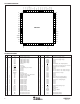
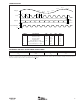
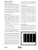
PIN CONFIGURATION REFBY GND IN GND IN GND GND GND GND REFT CM REFB GND 63 GND 64 +VSA TQFP +VSA Top View 62 61 60 59 58 57 56 55 54 53 52 51 50 49 +VSA 1 48 GND +VSA 2 47 GND +VSD 3 46 VREF +VSD 4 45 SEL1 +VSD 5 44 SEL2 +VSD 6 43 GND GND 7 42 GND GND 8 CLK 41 BTC ADS5421Y 9 40 PD CLK 10 39 OE GND 11 38 GNDRV 25 26 27 28 29 30 31 32 NC 24 NC 23 B14 (LSB) 22 B13 21 B12 20 B11 19 B10 18 B9 17 B8 33 VDRV B7 34 VDRV DV 16
TIMING DIAGRAM N+9 N+8 N+2 N+1 Analog In N+4 N+3 N tD N+5 tL tCONV N + 10 N+7 N+6 tH Clock 10 Clock Cycles t2 Data Out N – 10 N–9 N–8 N–7 N–6 N–5 N–4 N–3 N–2 N–1 Data Invalid N t1 Data Valid Output tDV SYMBOL t CONV tL tH tD t1 t2 tDV DESCRIPTION MIN Convert Clock Period Clock Pulse LOW Clock Pulse HIGH Aperture Delay Data Hold Time, CL = 0pF New Data Delay Time, CL = 15pF max 25 11.5 11.5 Data Valid Output, CL = 15pF 3.9 TYP MAX UNITS 1µs t CONV /2 t CONV /2 3 7.2 12.
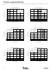
TYPICAL CHARACTERISTICS TA = 25°C, +VSA = +VSD = +5V, differential input range = 1.5V to 3.5V each input (4VPP), sampling rate = 40MSPS, internal reference, and VDRV = 3V, unless otherwise noted. SPECTRAL PERFORMANCE SPECTRAL PERFORMANCE 0 0 FIN = 1MHz, –1dBFS FIN = 10MHz, –1dBFS SFDR = 88.4dBFS –20 SFDR = 85dBFS –20 SNR = 74.5dBFS –40 Amplitude (dB) Amplitude (dB) SNR = 76.
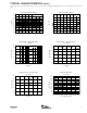
TYPICAL CHARACTERISTICS (Cont.) TA = 25°C, +VSA = +VSD = +5V, differential input range = 1.5V to 3.5V each input (4VPP), sampling rate = 40MSPS, internal reference, and VDRV = 3V, unless otherwise noted. DIFFERENTIAL LINEARITY ERROR 0.5 INTEGRAL LINEARITY ERROR 4 FIN = 1MHz 0.4 FIN = 1MHz 3 0.3 2 0.1 ILE (LSB) DLE (LSB) 0.2 0.0 –0.1 1 0 –1 –0.2 –2 –0.3 –3 –0.4 –0.
TYPICAL CHARACTERISTICS (Cont.) TA = 25°C, +VSA = +VSD = +5V, differential input range = 1.5V to 3.5V each input (4VPP), sampling rate = 40MSPS, internal reference, and VDRV = 3V, unless otherwise noted.
ANALOG INPUTS TYPES OF APPLICATIONS The analog input of the ADS5421 can be configured in various ways and driven with different circuits, depending on the application and the desired level of performance. Offering an extremely high dynamic range at high input frequencies, the ADS5421 is particularly well suited for communication systems that digitize wideband signals.
For applications that use op amps to drive the ADC, it is recommended that a series resistor be added between the amplifier output and the converter inputs. This will isolate the capacitive input of the converter from the driving source and avoid gain peaking, or instability; furthermore, it will create a 1st-order, low-pass filter in conjunction with the specified input capacitance of the ADS5421.
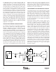
+5V VIN (IF) Optional Bandpass Filter RS IF Amplifier XFR 1:n RIN IN RT RIN CIN ADS5421 IN CM NOTE: Supply bypassing not shown. + 0.1µF 2.2µF FIGURE 4. Driving the ADS5421 with a Low-Distortion IF Amplifier and a Transformer Suited for IF Sampling Applications. TRANSFORMER-COUPLED, SINGLE-ENDED-TODIFFERENTIAL CONFIGURATION For applications in which the input frequency is limited to approximately 10MHz (e.g., baseband), a high-speed operational amplifier may be used.
AC-COUPLED, DIFFERENTIAL INTERFACE WITH GAIN sets a pole at approximately 85MHz and rolls off some of the wideband noise resulting in a reduction of the noise floor. The interface circuit example presented in Figure 6 employs two OPA687s, (decompensated voltage-feedback op amps), optimized for gains of 12V/V or higher. Implementing a new compensation technique allows the OPA847s to operate with a reduced signal gain of 8.
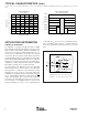
REFERENCE REFERENCE OPERATION Integrated into the ADS5421 is a bandgap reference circuit, including logic that provides a +1.5V or +2V reference output by selecting the corresponding pin-strap configuration. Table I lists an overview of the possible reference options and pin configurations. Figure 8 shows the basic model of the internal reference circuit.
+5V +5V 1/2 OPA2234 4.7kΩ REFT + R3 + 0.1µF ADS5421 R4 R1 REF1004 +2.5V 2.2µF 10µF 1/2 OPA2234 R2 REFB + 0.1µF 2.2µF 0.1µF FIGURE 9. Example for an External Reference Circuit Using a Dual, Single-Supply Op Amp. DIGITAL INPUTS AND OUTPUTS CLOCK INPUT CLK Unlike most ADCs, the ADS5421 contains internal clock conditioning circuitry. This enables the converter to adapt to a variety of application requirements and different clock sources.
MINIMUM SAMPLING RATE The clock inputs of the ADS5421 can be connected in a number of ways. However, the best performance is obtained when the clock input pins are driven differentially. Operating in this mode, the clock inputs accommodate signal swings ranging from 2.5VPP down to 0.5VPP differentially. This allows direct interfacing of clock sources such as voltage-controlled crystal oscillators (VCXO) to the ADS5421.
OUTPUT ENABLE (OE ) POWER DISSIPATION The digital outputs of the ADS5421 can be set to high impedance (tri-state), exercising the output enable pin (OE). For normal operation, this pin must be at a logic LOW potential, whereas a logic HIGH voltage disables the outputs. Even though this function affects the output driver stage, the threshold voltages for the OE pin do not depend on the output driver supply (VDRV), but are fixed (see the Electrical Characteristics Table and the Digital Inputs Sections).
VIN 50Ω ADT2-1 4.7µF + +VA (5V) 0.1µF 0.1µF 22Ω 22Ω 4.7µF + 4.7µF + 0.1µF 0.
LAYOUT AND DECOUPLING CONSIDERATIONS Proper grounding and bypassing, short lead length, and the use of ground planes are particularly important for highfrequency designs. Achieving optimum performance with a fast sampling converter like the ADS5421 requires careful attention to the PC board layout to minimize the effect of board parasitics and optimize component placement. A multilayer board usually ensures best results and allows convenient component placement.
Revision History DATE REVISION PAGE SECTION — — 1 Features 2 Electrical Characteristics Changed Optional Input Ranges to Optional Input Range and deleted 2Vp-p, same line under TYP. 3 Electrical Characteristics Changed External REF Voltage Range from 9.9V to 1.4V (minimum). Added (VREFT – VREFB) to ACCURACY section under CONDITIONS column.
PACKAGE OPTION ADDENDUM www.ti.
PACKAGE MATERIALS INFORMATION www.ti.com 14-Jul-2012 TAPE AND REEL INFORMATION *All dimensions are nominal Device ADS5421Y/T Package Package Pins Type Drawing LQFP PM 64 SPQ 250 Reel Reel A0 Diameter Width (mm) (mm) W1 (mm) 330.0 24.8 Pack Materials-Page 1 12.3 B0 (mm) K0 (mm) P1 (mm) W Pin1 (mm) Quadrant 12.3 2.5 16.0 24.
PACKAGE MATERIALS INFORMATION www.ti.com 14-Jul-2012 *All dimensions are nominal Device Package Type Package Drawing Pins SPQ Length (mm) Width (mm) Height (mm) ADS5421Y/T LQFP PM 64 250 367.0 367.0 45.
MECHANICAL DATA MTQF008A – JANUARY 1995 – REVISED DECEMBER 1996 PM (S-PQFP-G64) PLASTIC QUAD FLATPACK 0,27 0,17 0,50 0,08 M 33 48 49 32 64 17 0,13 NOM 1 16 7,50 TYP Gage Plane 10,20 SQ 9,80 12,20 SQ 11,80 0,25 0,05 MIN 0°– 7° 0,75 0,45 1,45 1,35 Seating Plane 0,08 1,60 MAX 4040152 / C 11/96 NOTES: A. B. C. D. All linear dimensions are in millimeters. This drawing is subject to change without notice.
IMPORTANT NOTICE Texas Instruments Incorporated and its subsidiaries (TI) reserve the right to make corrections, enhancements, improvements and other changes to its semiconductor products and services per JESD46C and to discontinue any product or service per JESD48B. Buyers should obtain the latest relevant information before placing orders and should verify that such information is current and complete.