
Datasheet
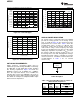


FSO
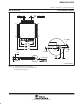
ADS1601
SCLK
DOUT
SYNC
FSR
TMS320
CLKR
DR
FSX
ADS1601
SBAS322D –DECEMBER 2004–REVISED OCTOBER 2011
www.ti.com
LAYOUT ISSUES AND COMPONENT The McBSP provides a host of functions including:
SELECTION
• Full-duplex communication
• Double-buffered data registers
The ADS1601 is a very high-speed, high-resolution
data converter. In order to achieve maximum
• Independent framing and clocking for reception
performance, the user must give very careful
and transmission of data
consideration to both the layout of the printed circuit
The sequence begins with a one-time synchronization
board (PCB) in addition to the routing of the traces.
of the serial port by the microprocessor. The
Capacitors that are critical to achieve the best
ADS1601 recognizes the SYNC signal if it is high for
performance from the device should be placed as
at least one CLK period. Transfers are initiated by the
close to the pins of the device as possible. These
ADS1601 after the SYNC signal is de-asserted by the
include capacitors related to the analog inputs, the
microprocessor.
reference, and the power supplies.
The FSO signal from the ADS1601 indicates that
For critical capacitors, it is recommended that Class II
data is available to be read, and is connected to the
dielectrics such as Z5U be avoided. These dielectrics
frame sync receive (FSR) pin of the DSP. The clock
have a narrow operating temperature, a large
receiver (CLKR) is derived directly from the ADS1601
tolerance on the capacitance, and lose up to 20% of
serial clock output to ensure continued
the rated capacitance over 10,000 hours. Rather,
synchronization of data with the clock.
select capacitors with a Class I dielectric. C0G (also
known as NP0), for example, has a tight tolerance
less than ±30ppm/°C and is very stable over time.
Should Class II capacitors be chosen because of the
size constraints, select an X7R or X5R dielectric to
minimize the variations of the capacitor’s critical
characteristics.
The resistors used in the circuits to drive the input
and reference should be kept as low as possible to
prevent excess thermal noise from degrading the
system performance.
The digital outputs from the device should always be
buffered. This will have a number of benefits: it
Figure 51. ADS1601—TMS320 Interface
reduces the loading of the internal digital buffers,
Connection
which decreases noise generated within the device,
and it also reduces device power consumption.
An evaluation module (EVM) is available from Texas
Instruments. The module consists of the ADS1601
APPLICATIONS INFORMATION
and supporting circuits, allowing users to quickly
assess the performance and characteristics of the
Interfacing the ADS1601 to the TMS320 DSP
ADS1601. The EVM easily connects to various
family.
microcontrollers and DSP systems. For more details,
Since the ADS1601 communicates with the host via a
or to download a copy of the ADS1601EVM User’s
serial interface, the most suitable method to connect
Guide, visit the Texas Instruments web site at
to any of the TMS320 DSPs is via the multi-channel
www.ti.com.
buffered serial port (McBSP). A typical connection to
the TMS320 DSP is shown in Figure 51.
22 Copyright © 2004–2011, Texas Instruments Incorporated