
Datasheet


C
P
C
P
C
P
C
P
C
P
C
P
C
P
C
P
1
36DGND
2
3
9
10
11
12
18
42 41
55 38 37 34 33
19
22
23
AVDD
AVDD
AGND
AGND
C
P
6
7 AVDD
AGND
AGND
AVDD
47 Fm
47 Fm
47 Fm 4.7 Fm 1 Fm 0.1 Fm
0.1 Fm
0.1 Fm
1 Fm
1 Fm
4.7 Fm
4.7 Fm
DVDD
AVDD
AGND
AGND
DGND
IOVDD
DVDD
DGND
DGND
15
10kW
RPULLUP
DGND
DVDD
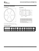
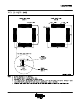
ADS1601
Ifusingseparateanalogand
digitalgroundplanes,connect
togetherontheADS1601PCB.
DGND
NOTE:C =
P
1 Fm úú m0.1 F
AGND
AVDD
IOVDD
DVDD
ADS1601
www.ti.com
SBAS322D –DECEMBER 2004–REVISED OCTOBER 2011
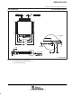
POWER DOWN (PD) POWER SUPPLIES
When not in use, the ADS1601 can be powered down Three supplies are used on the ADS1601: analog
by taking the PD pin low. All circuitry is shut down, (AVDD), digital (DVDD) and digital I/O (IOVDD). Each
including the voltage reference. To minimize the supply must be suitably bypassed to achieve the best
digital current during power down, stop the clock performance. It is recommended that a 1μF and
signal supplied to the CLK input. There is an internal 0.1μF ceramic capacitor be placed as close to each
pull-up resistor of 170kΩ on the PD pin, but it is supply pin as possible. Connect each supply-pin
recommended that this pin be connected to IOVDD if bypass capacitor to the associated ground, as shown
not used. Make sure to allow time for the reference to in Figure 50. Each main supply bus should also be
start up after exiting power-down mode. The internal bypassed with a bank of capacitors from 47μF to
reference typically requires 15ms. After the reference 0.1μF, as shown. The I/O and digital supplies (IOVDD
has stabilized, allow at least 100 conversions for the and DVDD) can be connected together when using
modulator and digital filter to settle before retrieving the same voltage. In this case, only one bank of 47μF
data. to 0.1μF capacitors is needed on the main supply
bus, though each supply pin must still be bypassed
with a 1μF and 0.1μF ceramic capacitor.
Figure 50. Recommended Power-Supply Bypassing
Copyright © 2004–2011, Texas Instruments Incorporated 21