
Datasheet


10 Fm
0.1 Fm
0.1 Fm
10 Fm 0.1 Fm
10 Fm
0.1 Fm
0.1 Fm
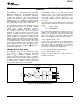
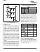
VREFP
VREFP
VMID
VCAP
VREFN
VREFN
392W
OPA2822
ADS1601
0.001 Fm
4V
392W
OPA2822
0.001 Fm
1V
392W
OPA2822
0.001 Fm
2.5V
AGND
+0.94V
2 1
REF
-
15
-0.94V
2 1
REF
-
15
-
REF
0.94V
2
2 1-
15
15
( )
£ -
REF
0.94V
2
2 1-
15
15
( )
ADS1601
SBAS322D –DECEMBER 2004–REVISED OCTOBER 2011
www.ti.com
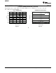
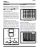
Table 1. Maximum Allowable Clock Source Jitter
for Different Input Signal Frequencies and
Amplitude
INPUT SIGNAL
MAXIMUM MAXIMUM MAXIMUM ALLOWABLE
FREQUENCY AMPLITUDE CLOCK SOURCE JITTER
500kHz –0.5dB 6ps
500kHz –20dB 60ps
100kHz –0.5dB 30ps
100kHz –20dB 300ps
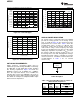
DATA FORMAT
The 16-bit output data are in binary two’s
complement format as shown in Table 2. When the
input is positive out-of-range, exceeding the positive
full-scale value of +0.94V
REF
, the output clips to all
7FFFh and the OTR output goes high.
Likewise, when the input is negative out-of-range by
going below the negative full-scale value
of –0.94V
REF
, the output clips to 8000h and the OTR
output goes high. The OTR remains high while the
input signal is out-of-range.
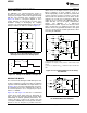
Figure 42. Recommended Buffer Circuit When
Using an External Reference
Table 2. Output Code versus Input Signal
INPUT SIGNAL (INP – IDEAL OUTPUT
CLOCK INPUT (CLK)
INN) CODE
(1)
OTR
≥ +0.94V
REF
(> 0dB) 7FFFh 1
The ADS1601 requires an external clock signal to be
–0.94V
REF
(0dB) 7FFFh 0
applied to the CLK input pin. The sampling of the
modulator is controlled by this clock signal. As with
001h 0
any high-speed data converter, a high quality clock is
essential for optimum performance. Crystal clock
0 0000h 0
oscillators are the recommended CLK source; other
sources, such as frequency synthesizers, are usually
FFFFh 0
inadequate. Make sure to avoid excess ringing on the
CLK input; keeping the trace as short as possible
helps.
8000h 0
Measuring high-frequency, large amplitude signals
requires tight control of clock jitter. The uncertainty
during sampling of the input from clock jitter limits the
8000h 1
maximum achievable SNR. This effect becomes more
pronounced with higher frequency and larger
(1) Excludes effects of noise, INL, offset and gain errors.
magnitude inputs. Fortunately, the ADS1601
oversampling topology reduces clock jitter sensitivity
OUT-OF-RANGE INDICATION (OTR)
over that of Nyquist rate converters such as pipeline
If the output code exceeds the positive or negative
and successive approximation converters by a factor
full-scale, the out-of-range digital output OTR will go
of √16.
high on the falling edge of SCLK. When the output
In order to not limit the ADS1601 SNR performance,
code returns within the full-scale range, OTR returns
keep the jitter on the clock source below the values
low on the falling edge of SCLK.
shown in Table 1. When measuring lower frequency
and lower amplitude inputs, more CLK jitter can be
tolerated. In determining the allowable clock source
jitter, select the worst-case input (highest frequency,
largest amplitude) that will be seen in the application.
18 Copyright © 2004–2011, Texas Instruments Incorporated