
Datasheet

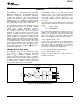


AINP+AINN
2
V =
CM
SD
Modulator
Digital
Filter
Serial
Interface
S
V
IN
VREFN IOVDDVREFP
V
REF
S
AINP
AINN
FSO
FSO
DOUT
DOUT
SCLK
SCLK
CLK
1.06
ADS1601
www.ti.com
SBAS322D –DECEMBER 2004–REVISED OCTOBER 2011
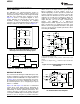
OVERVIEW
The ADS1601 is a high-performance delta-sigma The ADS1601 supports a very wide range of input
ADC. The modulator uses an inherently stable 2-1-1 signals. For V
REF
= 3V, the full-scale input voltage is
multi-stage architecture incorporating proprietary ±2.82V. Having such a wide input range makes
circuitry that allows for very linear high-speed out-of-range signals unlikely. However, if an
operation. The modulator samples the input signal at out-of-range signal occurs, the digital output OTR
20MSPS (when f
CLK
= 20MHz). A low-ripple linear goes high.
phase digital filter decimates the modulator output by
The analog inputs must be driven with a differential
16 to provide high resolution 16-bit output data.
signal to achieve optimum performance. For the input
Conceptually, the modulator and digital filter measure signal:
the differential input signal, V
IN
= (AINP – AINN),
against the scaled differential reference,
V
REF
= (VREFP – VREFN), as shown in Figure 35.
The voltage reference can either be generated
the recommended common-mode voltage is 2.7V. In
internally or supplied externally. A three-wire serial
addition to the differential and common-mode input
interface, designed for direct connection to DSPs,
voltages, the absolute input voltage is also important.
outputs the data. A separate power supply for the I/O
This is the voltage on either input (AINP or AINN)
allows flexibility for interfacing to different logic
with respect to AGND. The range for this voltage is:
families. Out-of-range conditions are indicated with a
–0.1V < (AINN or AINP) < 4.6V
dedicated digital output pin. Analog power dissipation
is controlled using an external resistor. This control
If either input is taken below –0.1V, ESD protection
allows reduced dissipation when operating at slower
diodes on the inputs will turn on. Exceeding 4.6V on
speeds. When not in use, power consumption can be
either input results in degradation in the linearity
dramatically reduced by setting the PD pin low to
performance. ESD protection diodes will also turn on
enter Power-Down mode.
if the inputs are taken above AVDD (+5V).
The recommended absolute input voltage is:
ANALOG INPUTS (AINP, AINN)
–0.1V < (AINN or AINP) < 4.2V
The ADS1601 measures the differential signal,
V
IN
= (AINP – AINN), against the differential
Keeping the inputs within this range provides for
reference, V
REF
= (VREFP – VREFN). The most
optimum performance.
positive measurable differential input is 0.94V
REF
,
which produces the most positive digital output code
of 7FFFh. Likewise, the most negative measurable
differential input is –0.94V
REF
, which produces the
most negative digital output code of 8000h.
Figure 35. Conceptual Block Diagram
Copyright © 2004–2011, Texas Instruments Incorporated 15