
Datasheet


"###$
SBAS282D − JUNE 2003 − REVISED MARCH 2004
www.ti.com
12
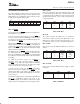
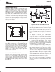
READING FROM THE ADS1112
To read the output register and the configuration register
from the ADS1112, first address the ADS1112 for reading,
then read three bytes. The first two bytes will be the output
register’s contents, and the third will be the configuration
register’s contents.
It is not required to read the configuration register byte. It
is permissible to read fewer than three bytes during a read
operation.
Reading more than three bytes from the ADS1112 has no
effect. All bytes following the third will be FF
H
.
It is possible to ignore the ST/DRDY
bit and read data from
the ADS1112 output register at any time, without regard to
whether a new conversion is complete. If the output
register is read more than once during a conversion cycle,
it will return the same data each time. New data will be
returned only when the output register has been updated.
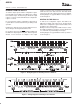
A timing diagram of a typical ADS1112 read operation is
shown in Figure 2.
WRITING TO THE ADS1112
To write to the configuration register, first address the
ADS1112 for writing, and send one byte. The byte will be
written to the configuration register. Note that data cannot
be written to the output register.
Writing more than one byte to the ADS1112 has no effect.
The ADS1112 will ignore any bytes sent to it after the first
one, and it will only acknowledge the first byte.
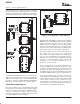
A timing diagram of a typical ADS1112 write operation is
shown in Figure 3.
Figure 2. Timing Diagram for Reading From the ADS1112
Figure 3. Timing Diagram for Writing To the ADS1112