
Datasheet


ADCS7476, ADCS7477, ADCS7478
www.ti.com
SNAS192F –APRIL 2003–REVISED MARCH 2013
The first solution to keeping digital noise out of the power supply is to decouple the supply from any other
components or use a separate supply for the ADC. To keep noise out of the supply, keep the output load
capacitance as small as practical. If the load capacitance is greater than 50 pF, use a 100 Ω series resistor at
the ADC output, located as close to the ADC output pin as practical. This will limit the charge and discharge
current of the output capacitance and improve noise performance. Since the series resistor and the load
capacitance form a low frequency pole, verify signal integrity once the series resistor has been added.
Power Management
When the ADCS7476/77/78 is operated continuously in normal mode, throughput up to 1 MSPS can be
achieved. The user may trade throughput for power consumption by simply performing fewer conversions per
unit time, and putting the ADCS7476/77/78 into shutdown mode between conversions. This method is not
advantageous beyond 350 kSPS throughput.
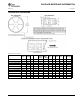
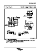
A plot of maximum power consumption versus throughput is shown in Figure 34. To calculate the power
consumption for a given throughput, remember that each time the part exits shutdown mode and enters normal
mode, one dummy conversion is required. Generally, the user will put the part into normal mode, execute one
dummy conversion followed by one valid conversion, and then put the part back into shutdown mode. When this
is done, the fraction of time spent in normal mode may be calculated by multiplying the throughput (in samples
per second) by 2 µs, the time taken to perform one dummy and one valid conversion. The power consumption
can then be found by multiplying the fraction of time spent in normal mode by the normal mode power
consumption figure. The power dissipated while the part is in shutdown mode is negligible.
For example, to calculate the power consumption at 300 kSPS with V
DD
= 5V, begin by calculating the fraction of
time spent in normal mode: 300,000 samples/second x 2 µs = 0.6, or 60%. The power consumption at 300 kSPS
is then 60% of 17.5 mW (the maximum power consumption at V
DD
= 5V) or 10.5 mW.
Figure 34. Maximum Power Consumption vs. Throughput
LAYOUT AND GROUNDING
Capacitive coupling between noisy digital circuitry and sensitive analog circuitry can lead to poor performance.
The solution is to keep the analog and digital circuitry separated from each other and the clock line as short as
possible.
Digital circuits create substantial supply and ground current transients. This digital noise could have significant
impact upon system noise performance. To avoid performance degradation of the ADCS7476/77/78 due to
supply noise, do not use the same supply for the ADCS7476/77/78 that is used for digital logic.
Generally, analog and digital lines should cross each other at 90° to avoid crosstalk. However, to maximize
accuracy in high resolution systems, avoid crossing analog and digital lines altogether. It is important to keep
clock lines as short as possible and isolated from ALL other lines, including other digital lines. In addition, the
clock line should also be treated as a transmission line and be properly terminated.
Copyright © 2003–2013, Texas Instruments Incorporated Submit Documentation Feedback 21
Product Folder Links: ADCS7476 ADCS7477 ADCS7478