
Datasheet


ADCS7476, ADCS7477, ADCS7478
www.ti.com
SNAS192F –APRIL 2003–REVISED MARCH 2013
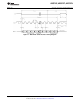
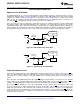
Sixteen SCLK cycles are required to read a complete sample from the ADCS7476/77/78. The sample bits
(including any leading or trailing zeroes) are clocked out on falling edges of SCLK, and are intended to be
clocked in by a receiver on subsequent falling edges of SCLK. The ADCS7476/77/78 will produce four leading
zeroes on SDATA, followed by twelve, ten, or eight data bits, most significant first. After the data bits, the
ADCS7477 will clock out two trailing zeros, and the ADCS7478 will clock out four trailing zeros. The ADCS7476
will not clock out any trailing zeros; the least significant data bit will be valid on the 16th falling edge of SCLK.
Depending upon the application, the first edge on SCLK after CS goes low may be either a falling edge or a
rising edge. If the first SCLK edge after CS goes low is a rising edge, all four leading zeroes will be valid on the
first four falling edges of SCLK. If instead the first SCLK edge after CS goes low is a falling edge, the first leading
zero may not be set up in time for a microprocessor or DSP to read it correctly. The remaining data bits are still
clocked out on the falling edges of SCLK.
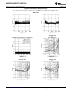
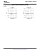
ADCS7476/77/78 TRANSFER FUNCTION
The output format of the ADCS7476/77/78 is straight binary. Code transitions occur midway between successive
integer LSB values. The LSB widths for the ADCS7476 is V
DD
/ 4096; for the ADCS7477 the LSB width is V
DD
/
1024; for the ADCS7478, the LSB width is V
DD
/ 256. The ideal transfer characteristic for the ADCS7476 and
ADCS7477 is shown in Figure 28, while the ideal transfer characteristic for the ADCS7478 is shown in Figure 29.
Figure 28. ADCS7476/77 Ideal Transfer Characteristic
Figure 29. ADCS7478 Ideal Transfer Characteristic
Copyright © 2003–2013, Texas Instruments Incorporated Submit Documentation Feedback 17
Product Folder Links: ADCS7476 ADCS7477 ADCS7478