
Datasheet


Table Of Contents
- Features
- Applications
- Key Specifications
- Description
- Absolute Maximum Ratings
- Operating Ratings
- Package Thermal Resistance
- Converter Characteristics
- DC Electrical Characteristics
- AC Electrical Characteristics
- TRI-STATE Test Circuits and Waveforms
- Typical Performance Characteristics
- Functional Description
- Revision History
ADC10662, ADC10664
www.ti.com
SNAS076E –JUNE 1999–REVISED MARCH 2013
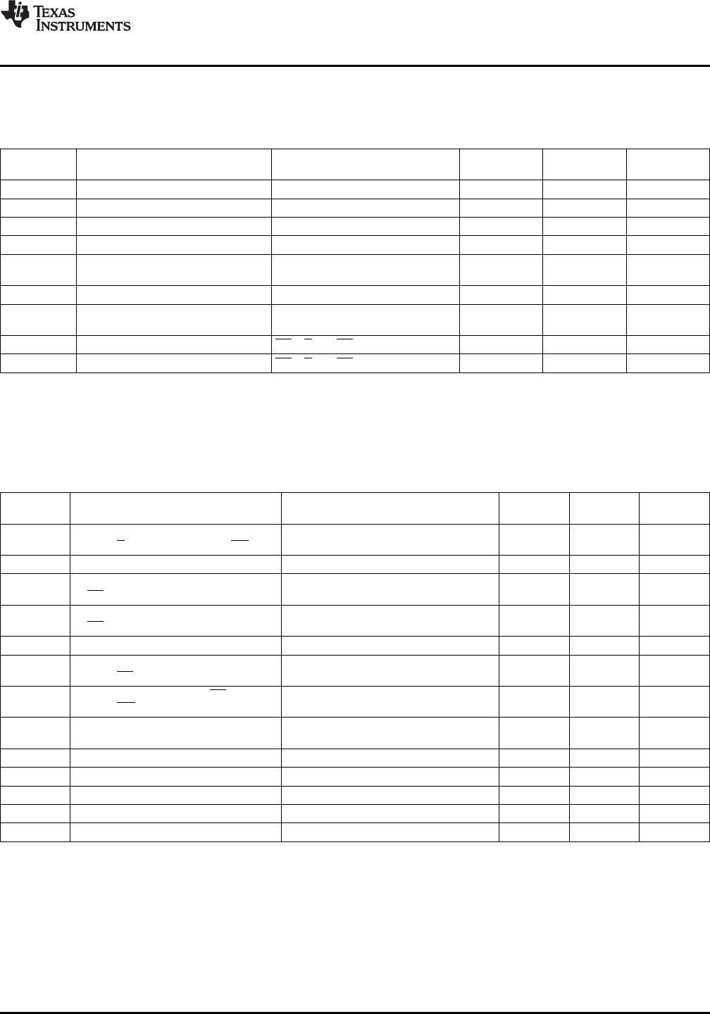
DC Electrical Characteristics
The following specifications apply for V
+
= +5V, V
REF(+)
= 5V V
REF(−)
= GND, and Speed Adjust pin connected to ground
through a 14.0 kΩ resistor (Mode 1) or an 8.26 kΩ resistor (Mode 2) unless otherwise specified. Boldface limits apply for T
A
= T
J
= T
MIN
to T
MAX
; all other limits T
A
= T
J
= +25°C.
Units
Symbol Parameter Conditions Typical
(1)
Limit
(2)
(Limits)
V
IN(1)
Logical “1” Input Voltage V
+
= 5.5V 2.0 V (min)
V
IN(0)
Logical “0” Input Voltage V
+
= 4.5V 0.8 V (max)
I
IN(1)
Logical “1” Input Current V
IN(1)
= 5V 0.005 3.0 μA (max)
I
IN(0)
Logical “0” Input Current V
IN(0)
0V −0.005 −3.0 μA (max)
V
+
= 4.5V, I
OUT
= −360 μA 2.4 V (min)
V
OUT(1)
Logical “1” Output Voltage
V
+
= 4.5V, I
OUT
= −10 μA 4.25 V (min)
V
OUT(0)
Logical “0” Output Voltage V
+
= 4.5V, I
OUT
= 1.6 mA 0.4 V (max)
V
OUT
= 5V 0.1 50 μA (max)
I
OUT
TRI-STATE Output Current
V
OUT
= 0V −0.1 −50 μA (max)
DI
CC
DV
CC
Supply Current CS = S/H = RD = 0 1.0 2 mA (max)
AI
CC
AV
CC
Supply Current CS = S/H = RD = 0 30 45 mA (max)
(1) Typical figures represent most likely parametric norm.
(2) Tested limits are ensured to AOQL (Average Outgoing Quality Level).
AC Electrical Characteristics
The following specifications apply for V
+
= +5V, t
r
= t
f
= 20 ns, V
REF(+)
= 5V, V
REF(−)
= GND, and Speed Adjust pin connected to
ground through a 14.0 kΩ resistor (Mode 1) or an 8.26 kΩ resistor (Mode 2) unless otherwise specified. Boldface limits
apply for T
A
= T
J
= T
MIN
to T
MAX
; all other limits T
A
= T
J
= +25°C.
Units
Symbol Parameter Conditions Typical
(1)
Limit
(2)
(Limits)
Mode 1 Conversion Time from Rising
t
CONV
360 466 ns (max)
Edge of S/H to Falling Edge of INT
t
CRD
Mode 2 Conversion Time 470 610 ns (max)
Access Time (Delay from Falling Edge
t
ACC1
Mode 1; C
L
= 100 pF 30 50 ns (max)
of RD to Output Valid)
Access Time (Delay from Falling Edge
t
ACC2
Mode 2; C
L
= 100 pF 475 616 ns (max)
of RD to Output Valid)
t
SH
Minimum Sample Time Mode 1 (Figure 3)
(3)
150 ns (max)
TRI-STATE Control (Delay from Rising
t
1H
, t
0H
R
L
= 1k, C
L
= 10 pF 30 60 ns (max)
Edge of RD to High-Z State)
Delay from Rising Edge of RD to Rising
t
INTH
C
L
= 100 pF 25 50 ns (max)
Edge of INT
Delay from End of Conversion to Next
t
P
50 ns (max)
Conversion
t
MS
Multiplexer Control Setup Time 10 75 ns (max)
t
MH
Multiplexer Hold Time 10 40 ns (max)
C
VIN
Analog Input Capacitance 35 pF (max)
C
OUT
Logic Output Capacitance 5 pF (max)
C
IN
Logic Input Capacitance 5 pF (max)
(1) Typical figures represent most likely parametric norm.
(2) Tested limits are ensured to AOQL (Average Outgoing Quality Level).
(3) Accuracy may degrade if t
SH
is shorter than the value specified. See curves of Accuracy vs. t
SH
.
Copyright © 1999–2013, Texas Instruments Incorporated Submit Documentation Feedback 5
Product Folder Links: ADC10662 ADC10664