
Datasheet


Table Of Contents
- Features
- Applications
- Key Specifications
- Description
- Absolute Maximum Ratings
- Operating Ratings
- Package Thermal Resistance
- Converter Characteristics
- DC Electrical Characteristics
- AC Electrical Characteristics
- TRI-STATE Test Circuits and Waveforms
- Typical Performance Characteristics
- Functional Description
- Revision History
ADC10662, ADC10664
SNAS076E –JUNE 1999–REVISED MARCH 2013
www.ti.com
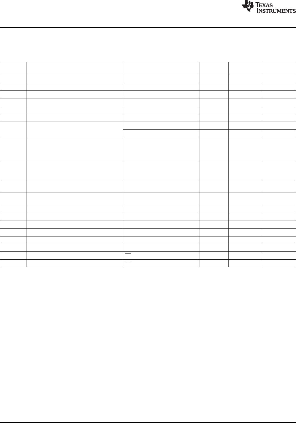
Converter Characteristics
The following specifications apply for V
+
= +5V, V
REF(+)
= +5V, V
REF(−)
= GND, and Speed Adjust pin connected to ground
through a 14.0 kΩ resistor (Mode 1) or an 8.26 kΩ resistor (Mode 2) unless otherwise specified. Boldface limits apply for T
A
= T
J
= T
Min
to T
Max
; all other limits T
A
= T
J
= +25°C.
Units
Symbol Parameter Conditions Typical
(1)
Limit
(2)
(Limit)
Resolution 10 Bits
Integral Linearity Error ±0.5 ±1.0/±1.5 LSB (max)
Offset Error ±1.5 LSB (max)
Full-Scale Error ±1 LSB (max)
Total Unadjusted Error ±0.5 ±1.5/±2.2 LSB
Missing Codes 0 (max)
V
+
= 5V ±5%, V
REF
= 4.5V ±1/16 LSB
Power Supply Sensitivity
V
+
= 5V ±10%, V
REF
= 4.5V ±⅛ LSB
f
IN
= 1 kHz, 4.85 V
P-P
−68 dB
f
IN
= 50 kHz, 4.85 V
P-P
−66 −60 dB (max)
THD Total Harmonic Distortion
(3)
f
IN
= 100 kHz, 4.85 V
P-P
−62 dB
f
IN
= 240 kHz, 4.85 V
P-P
−58 dB
f
IN
= 1 kHz, 4.85 V
P-P
61 dB
SNR Signal-to-Noise Ratio
(3)
f
IN
= 50 kHz, 4.85 V
P-P
60 58 dB (min)
f
IN
= 100 kHz, 4.85 V
P-P
60 dB
f
IN
= 1 kHz, 4.85 V
P-P
9.6 Bits
ENOB Effective Number of Bits
(3)
f
IN
= 50 kHz, 4.85 V
P-P
9.5 9 Bits (min)
400 Ω (min)
R
REF
Reference Resistance 650
900 Ω (max)
V
REF(+)
V
REF(+)
Input Voltage V
+
+ 0.05 V (max)
V
REF(−)
V
REF(−)
Input Voltage GND − 0.05 V (min)
V
REF(+)
V
REF(+)
Input Voltage V
REF(−)
V (min)
V
REF(−)
V
REF(−)
Input Voltage V
REF(+)
V (max)
V
IN
Input Voltage V
+
+ 0.05 V (max)
V
IN
Input Voltage GND − 0.05 V (min)
OFF Channel Input Leakage Current CS = V
+
, V
IN
= V
+
0.01 3 μA (max)
ON Channel Input Leakage Current CS = V
+
, V
IN
= V
+
±1 −3 μA (max)
(1) Typical figures represent most likely parametric norm.
(2) Tested limits are ensured to AOQL (Average Outgoing Quality Level).
(3) THD, SNR, and ENOB are tested in Mode 1. Measuring these quantities in Mode 2 yields similar values.
4 Submit Documentation Feedback Copyright © 1999–2013, Texas Instruments Incorporated
Product Folder Links: ADC10662 ADC10664