
Datasheet


Table Of Contents
- Features
- Applications
- Key Specifications
- Description
- Absolute Maximum Ratings
- Operating Ratings
- Package Thermal Resistance
- Converter Characteristics
- DC Electrical Characteristics
- AC Electrical Characteristics
- TRI-STATE Test Circuits and Waveforms
- Typical Performance Characteristics
- Functional Description
- Revision History
ADC10662, ADC10664
www.ti.com
SNAS076E –JUNE 1999–REVISED MARCH 2013
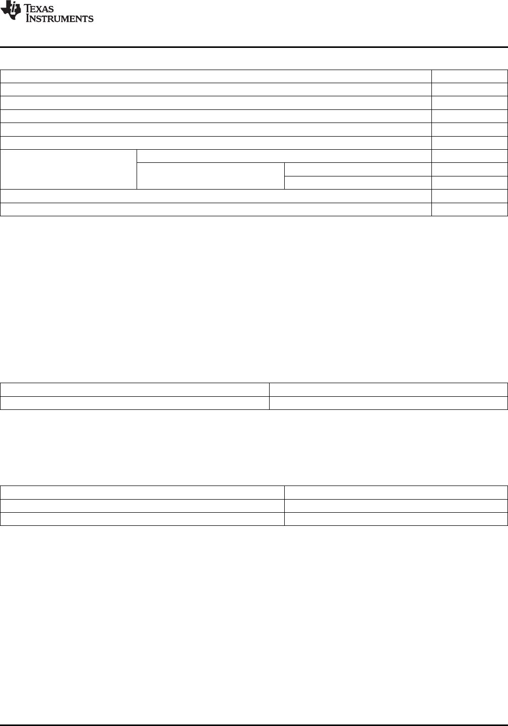
Absolute Maximum Ratings
(1)(2)(3)
Supply Voltage (V
+
= AV
CC
= DV
CC
) −0.3V to +6V
Voltage at Any Input or Output −0.3V to V
+
+ 0.3V
Input Current at Any Pin
(4)
5 mA
Package Input Current
(4)
20 mA
Power Dissipation
(5)
875 mW
ESD Susceptibility
(6)
2000V
N Package (10 Sec) 260°C
Soldering Information Vapor Phase (60 Sec) 215°C
SOIC Package
Infrared (15 Sec) 220°C
Storage Temperature Range −65°C to +150°C
Junction Temperature 150°C
(1) All voltages are measured with respect to GND, unless otherwise specified.
(2) Absolute Maximum Ratings indicate limits beyond which damage to the device may occur. Operating Ratings indicate conditions for
which the device is functional. These ratings do not ensure specific performance limits, however. For ensured specifications and test
conditions, see the Electrical Characteristics. The specified specifications apply only for the test conditions listed. Some performance
characteristics may degrade when the device is not operated under the listed test conditions.
(3) If Military/Aerospace specified devices are required, please contact the Texas Instruments Sales Office/Distributors for availability and
specifications.
(4) When the input voltage (V
IN
) at any pin exceeds the power supply rails (V
IN
< GND or V
IN
> V
+
) the absolute value of current at that pin
should be limited to 5 mA or less. The 20 mA package input current limits the number of pins that can safely exceed the power supplies
with an input current of 5 mA to four.
(5) The maximum power dissipation must be derated at elevated temperatures and is dictated by T
JMAX
, θ
JA
and the ambient temperature,
T
A
. The maximum allowable power dissipation at any temperature is P
D
= (T
JMAX
− T
A
)/θ
JA
or the number given in the Absolute
Maximum Ratings, whichever is lower. In most cases, the maximum derated power dissipation will be reached only during fault
conditions. For these devices, T
JMAX
for a board-mounted device can be found in Package Thermal Resistance.
(6) Human body model, 100 pF discharged through a 1.5 kΩ resistor.
Operating Ratings
(1)(2)
Temperature Range T
MIN
≤ T
A
≤ T
MAX
= −40°C ≤ T
A
≤ +85°C
Supply Voltage Range +4.5V to +5.5V
(1) Absolute Maximum Ratings indicate limits beyond which damage to the device may occur. Operating Ratings indicate conditions for
which the device is functional. These ratings do not ensure specific performance limits, however. For ensured specifications and test
conditions, see the Electrical Characteristics. The specified specifications apply only for the test conditions listed. Some performance
characteristics may degrade when the device is not operated under the listed test conditions.
(2) All voltages are measured with respect to GND, unless otherwise specified.
Package Thermal Resistance
Device θ
JA
(°C/W)
ADC10662CIWM 82
ADC10664CIWM 78
Copyright © 1999–2013, Texas Instruments Incorporated Submit Documentation Feedback 3
Product Folder Links: ADC10662 ADC10664