
Datasheet


Table Of Contents
- Features
- Applications
- Key Specifications
- Description
- Absolute Maximum Ratings
- Operating Ratings
- Package Thermal Resistance
- Converter Characteristics
- DC Electrical Characteristics
- AC Electrical Characteristics
- TRI-STATE Test Circuits and Waveforms
- Typical Performance Characteristics
- Functional Description
- Revision History
ADC10662, ADC10664
SNAS076E –JUNE 1999–REVISED MARCH 2013
www.ti.com
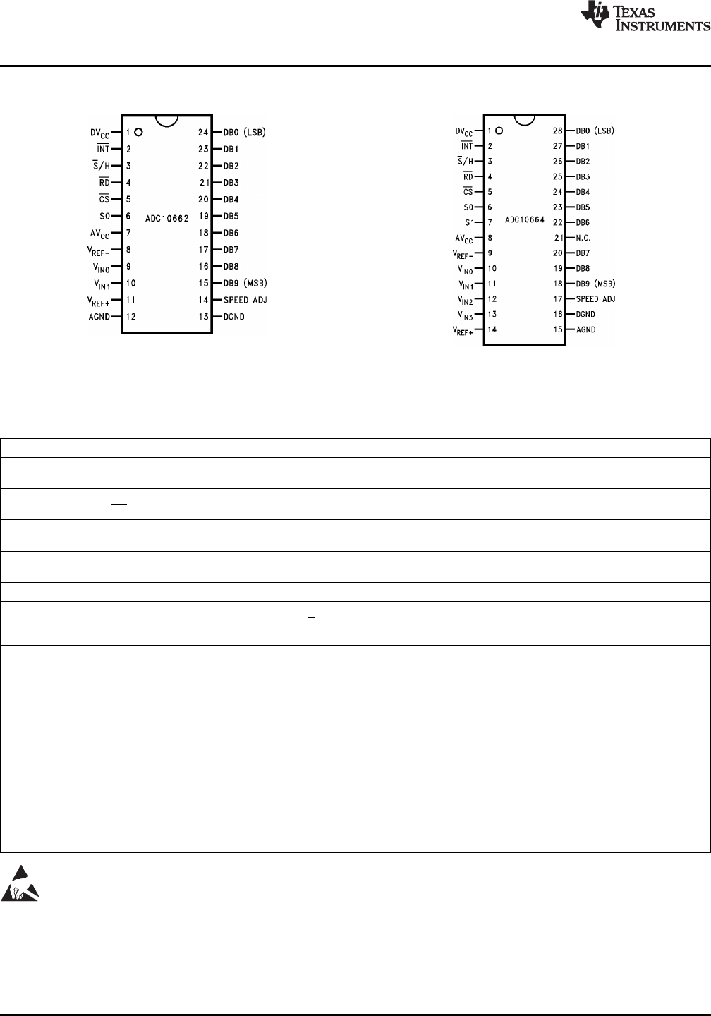
Connection Diagram
Figure 1. Top View Figure 2. Top View
NOTE: The ADC10662 is obsolete; shown for reference only.
PIN DESCRIPTIONS
Pin Function Description
DV
CC
, AV
CC
Digital and analog positive supply voltage inputs. Connect both to the same voltage source, but bypass separately with
a 0.1 µF ceramic capacitor in parallel with a 10 µF tantalum capacitor to ground at each pin.
INT Active low interrupt output. INT goes low at the end of each conversion, and returns high following the rising edge of
RD .
S/H Sample/Hold control input. When this pin is forced low (and CS is low), the analog input signal to be sampled and
initiates a new conversion.
RD Active low Read control input. When this RD and CS are low, any data present in the output registers will be placed on
the data bus.
CS Active low Chip Select control input. When low, this pin enables the RD and S/H pins.
S0, S1 These pins select the analog input that will be connected to the A/D during the conversion. The input is selected
based on the state of S0 and S1 when S/H makes its High-to-Low transition (See Timing Diagrams). The ADC10664
includes both S0 and S1. The ADC10662 includes just S0.
V
REF−
, V
REF+
Reference voltage inputs. They may be placed at any voltage between GND and V
CC
, but V
REF+
must be greater than
V
REF−
. An input voltage equal to V
REF−
produces an output code of 0, and an input voltage equal to (V
REF+
− 1 LSB)
produces an output code of 1023.
V
IN0
, V
IN1
, V
IN2
, Analog input pins. The ADC10662 has two inputs (V
IN0
and V
IN1
) and the ADC10664 has four inputs (V
IN0
, V
IN1
, V
IN2
V
IN3
and V
IN3
). The impedance of the source should be less than 500Ω for best accuracy and conversion speed. For
accurate conversions, no input pin (even one that is not selected) should be driven more than 50 mV above V
CC
or 50
mV below ground.
GND, AGND, Power supply ground pins. The ADC10662 and ADC10664 have separate analog and digital ground pins (AGND and
DGND DGND) for separate bypassing of the analog and digital supplies. The ground pins should be connected to a stable,
noise-free system ground. Both pins should be returned to the same potential.
DB0–DB9 TRI-STATE output pins.
SPEEDADJ By connecting a resistor between this pin and ground, the conversion time can be reduced. The specifications listed in
the table of Electrical Characteristics apply for a speed adjust resistor (R
SA
) equal to 14.0 kΩ (Mode 1) or 8.26 kΩ
(Mode 2). See Typical Performance Characteristics and the table of Electrical Characteristics.
These devices have limited built-in ESD protection. The leads should be shorted together or the device placed in conductive foam
during storage or handling to prevent electrostatic damage to the MOS gates.
2 Submit Documentation Feedback Copyright © 1999–2013, Texas Instruments Incorporated
Product Folder Links: ADC10662 ADC10664