
Datasheet


Table Of Contents
- Features
- Applications
- Key Specifications
- Description
- Absolute Maximum Ratings
- Operating Ratings
- Package Thermal Resistance
- Converter Characteristics
- DC Electrical Characteristics
- AC Electrical Characteristics
- TRI-STATE Test Circuits and Waveforms
- Typical Performance Characteristics
- Functional Description
- Revision History
ADC10662, ADC10664
SNAS076E –JUNE 1999–REVISED MARCH 2013
www.ti.com
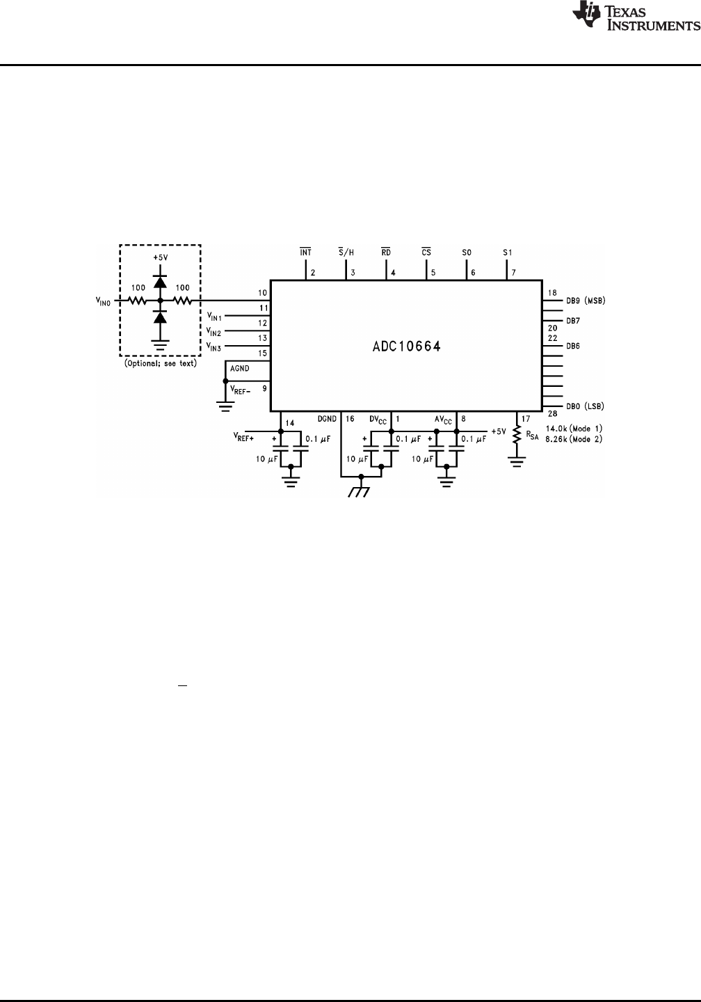
Correct conversion results will be obtained for input voltages greater than GND − 50 mV and less than V
+
+
50 mV. Do not allow the signal source to drive the analog input pin beyond the Absolute Maximum Rating. If an
analog input pin is forced beyond these voltages, the current flowing through the pin should be limited to 5 mA or
less to avoid permanent damage to the IC. The sum of all the overdrive currents into all pins must be less than
the Absolute Maximum Rating for Package Input Current. When the input signal is expected to extend beyond
this limit, an input protection scheme should be used. A simple input protection network using diodes and
resistors is shown in Figure 20. Note the multiple bypass capacitors on the reference and power supply pins. If
V
REF−
is not grounded, it should also be bypassed to analog ground using multiple capacitors (see POWER
SUPPLY CONSIDERATIONS). AGND and DGND should be at the same potential. V
IN0
is shown with an input
protection network.
Figure 20. Typical Connection
INHERENT SAMPLE-AND-HOLD
Because the ADC10662 and ADC10664 sample the input signal once during each conversion, they are capable
of measuring relatively fast input signals without the help of an external sample-hold. In a non-sampling
successive-approximation A/D converter, regardless of speed, the input signal must be stable to better than ±1/2
LSB during each conversion cycle or significant errors will result. Consequently, even for many relatively slow
input signals, the signals must be externally sampled and held constant during each conversion if a SAR with no
internal sample-and-hold is used.
Because they incorporate a direct sample/hold control input, the ADC10662 and ADC10664 are suitable for use
in DSP-based systems. The S/H input allows synchronization of the A/D converter to the DSP system's sampling
rate and to other ADC10662s, and ADC10664s.
POWER SUPPLY CONSIDERATIONS
The ADC10662 and ADC10664 are designed to operate from a +5V (nominal) power supply. There are two
supply pins, AV
CC
and DV
CC
. These pins allow separate external bypass capacitors for the analog and digital
portions of the circuit. To ensure accurate conversions, the two supply pins should be connected to the same
voltage source, and each should be bypassed with a 0.1 μF ceramic capacitor in parallel with a 10 μF tantalum
capacitor. Depending upon the circuit board layout and other system considerations, more bypassing may be
necessary.
The ADC10662 and ADC10664 have separate analog and digital ground pins for separate bypassing of the
analog and digital supplies. Their ground pins should be connected to the same potential, and all grounds should
be “clean” and free of noise.
In systems with multiple power supplies, careful attention to power supply sequencing may be necessary to avoid
over-driving inputs. The A/D converter's power supply pins should be at the proper voltage before digital or
analog signals are applied to any of the other pins.
14 Submit Documentation Feedback Copyright © 1999–2013, Texas Instruments Incorporated
Product Folder Links: ADC10662 ADC10664