
Datasheet


Table Of Contents
ADC10040
SNAS224M –JULY 2003–REVISED APRIL 2013
www.ti.com
AC Electrical Characteristics
Unless otherwise specified, the following specifications apply for V
SSA
= V
SSIO
= 0V, V
DDA
= +3.0V, V
DDIO
= +2.5V, V
IN
= 2 V
P-P
(full scale), STBY = 0V, External V
REF
= 1.20V, f
CLK
= 40 MHz, 50% Duty Cycle, C
L
= 10 pF/pin. Boldface limits apply for T
A
= T
MIN
to T
MAX
: all other limits T
A
= 25°C
(1)(2)(3)
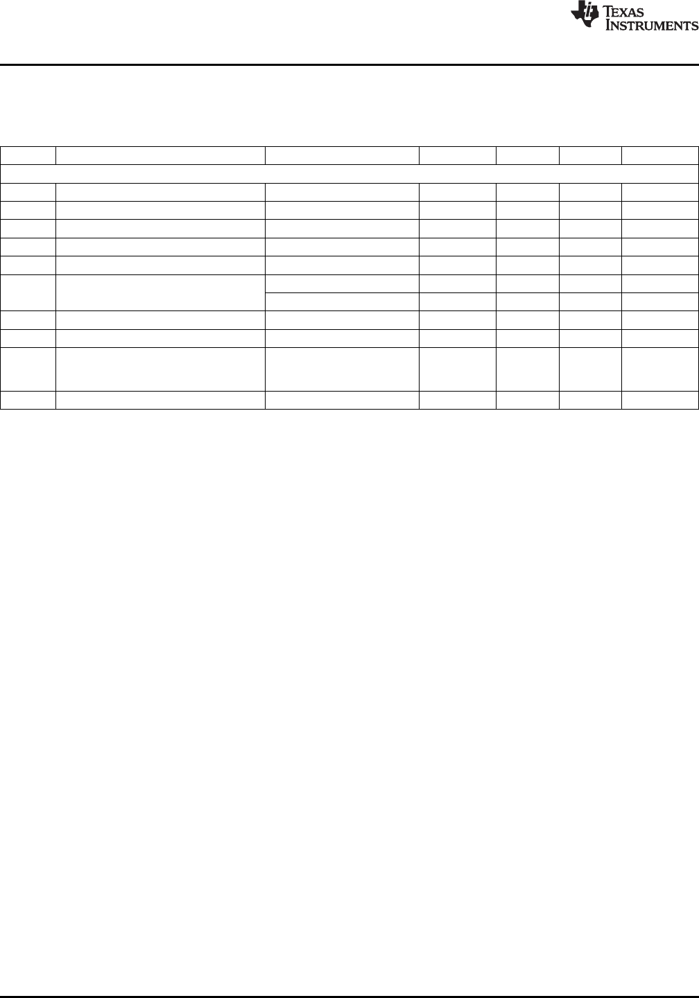
Symbol Parameter Conditions Min
(3)
Typ
(3)
Max
(3)
Units
CLK, DF, STBY, SENSE
f
CLK
1 Maximum Clock Frequency 40 MHz (min)
f
CLK
2 Minimum Clock Frequency 20 MHz
t
CH
Clock High Time 12.5 ns
t
CL
Clock Low Time 12.5 ns
t
CONV
Conversion Latency 6 Cycles
T = 25°C 2 3.3 5 ns
Data Output Delay after a Rising Clock
t
OD
Edge
1 6 ns
t
AD
Aperture Delay 1 ns
t
AJ
Aperture Jitter 2 ps (RMS)
Differential V
IN
step from ±3V
Over Range Recovery Time to 0V to get accurate 1 Clock Cycle
conversion
t
STBY
Standby Mode Exit Cycle 20 Cycles
(1) With the test condition for 2 V
P-P
differential input, the 10-bit LSB is 1.95 mV.
(2) Typical figures are at T
A
= T
J
= 25°C and represent most likely parametric norms. Test limits are ensured to TI's AOQL (Average
Outgoing Quality Level).
(3) Timing specifications are tested at TTL logic levels, V
IL
= 0.4V for a falling edge, and V
IH
= 2.4V for a rising edge.
8 Submit Documentation Feedback Copyright © 2003–2013, Texas Instruments Incorporated
Product Folder Links: ADC10040