
Datasheet


Table Of Contents
ADC10040
SNAS224M –JULY 2003–REVISED APRIL 2013
www.ti.com
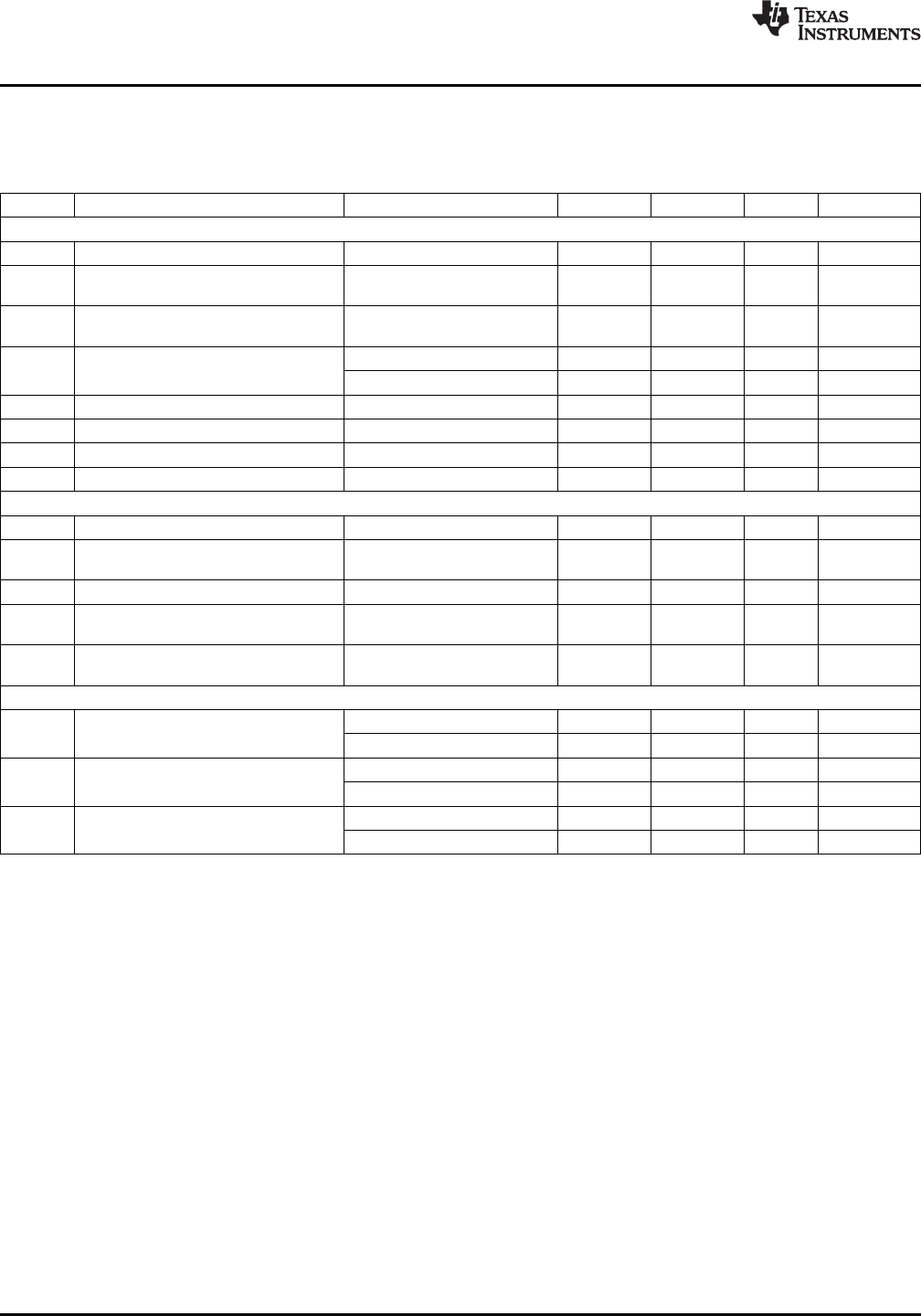
Converter Electrical Characteristics
Unless otherwise specified, the following specifications apply for V
SSA
= V
SSIO
= 0V, V
DDA
= +3.0V, V
DDIO
= +2.5V, V
IN
= 2 V
P-P
,
STBY = 0V, External V
REF
= 1.20V, f
CLK
= 40 MHz, 50% Duty Cycle, C
L
= 10 pF/pin. Boldface limits apply for T
A
= T
MIN
to
T
MAX
: all other limits T
A
= 25°C.
(1)(2)(3)
Symbol Parameter Conditions Min Typ Max Units
STATIC CONVERTER CHARACTERISTICS
No Missing Codes Ensured 10 Bits
F
IN
= 250 kHz, −0 dB Full
INL Integral Non-Linearity −1.0 ±0.3 +1.0 LSB
Scale
F
IN
= 250 kHz, −0 dB Full
DNL Differential Non-Linearity −0.9 ±0.3 +0.9 LSB
Scale
Positive Error −1.5 +0.4 +1.9 % FS
GE Gain Error
Negative Error −1.5 −0.01 +1.9 % FS
OE Offset Error (V
IN
+ = V
IN
−) −1.4 0.12 +1.6 % FS
Under Range Output Code 0
Over Range Output Code 1023
FPBW Full Power Bandwidth
(4)
400 MHz
REFERENCE AND INPUT CHARACTERISTICS
V
CM
Common Mode Input Voltage 0.5 1.5 V
Output Voltage for use as an input
V
COM
1.45 V
common mode voltage
(5)
V
REF
Reference Voltage 1.2 V
V
REFTC
Reference Voltage Temperature
±80 ppm/°C
Coefficient
C
IN
V
IN
Input Capacitance (each pin to
4 pF
V
SSA
)
POWER SUPPLY CHARACTERISTICS
STBY = 1 4.5 6.0 mA
I
VDDA
Analog Supply Current
STBY = 0 18 25 mA
STBY = 1, f
IN
= 0 Hz 0 mA
I
VDDIO
Digital Supply Current
(6)
STBY = 0, f
IN
= 0 Hz 0.6 0.8 mA
STBY = 1 13.5 18 mW
PWR Power Consumption
(7)
STBY = 0 55.5 77 mW
(1) To ensure accuracy, it is required that |V
DDA
–V
DDIO
| ≤ 100 mV and separate bypass capacitors are used at each power supply pin.
(2) With the test condition for 2 V
P-P
differential input, the 10-bit LSB is 1.95 mV.
(3) Typical figures are at T
A
= T
J
= 25°C and represent most likely parametric norms. Test limits are ensured to TI's AOQL (Average
Outgoing Quality Level).
(4) The input bandwidth is limited using a capacitor between V
IN
−
and V
IN
+
.
(5) V
COM
is a typical value, measured at room temperature. It is not ensured by test. Do not load this pin.
(6) V
DDIO
is the current consumed by the switching of the output drivers and is primarily determined by load capacitance on the output pins,
the supply voltage, V
DR
, and the rate at which the outputs are switching (which is signal dependent). I
DR
= V
DR
x (C
0
x f
0
+ C
1
x f
1
+ C
2
+ f
2
+....C
11
x f
11
) where V
DR
is the output driver supply voltage, C
n
is the total load capacitance on the output pin, and f
n
is the average
frequency at which the pin is toggling.
(7) Power consumption includes output driver power. (f
IN
= 0 MHz).
6 Submit Documentation Feedback Copyright © 2003–2013, Texas Instruments Incorporated
Product Folder Links: ADC10040