
Datasheet


Table Of Contents
ADC10040
SNAS224M –JULY 2003–REVISED APRIL 2013
www.ti.com
Pin Descriptions and Equivalent Circuits (continued)
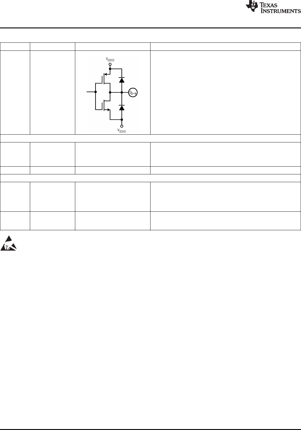
Pin No. Symbol Equivalent Circuit Description
16–20, Digital output data. D0 is the LSB and D9 is the MSB of the binary
D0–D9
23–27 output word.
ANALOG POWER
Positive analog supply pins. These pins should be connected to a
quiet 3,0V source and bypassed to analog ground with a 0.1 µF
2, 9, 10 V
DDA
monolithic capacitor located within 1 cm of these pins. A 4.7 µF
capacitor should also be used in parallel.
3, 11, 14 V
SSA
Ground return for the analog supply.
DIGITAL POWER
Positive digital supply pins for the ADC10040’s output drivers. This
pin should be bypassed to digital ground with a 0.1 µF monolithic
22 V
DDIO
capacitor located within 1 cm of this pin. A 4.7 µF capacitor should
also be used in parallel. The voltage on this pin should never exceed
the voltage on V
DDA
by more than 300 mV.
The ground return for the digital supply for the output drivers. This
21 V
SSIO
pin should be connected to the ground plane, but not near the
analog circuitry.
These devices have limited built-in ESD protection. The leads should be shorted together or the device placed in conductive foam
during storage or handling to prevent electrostatic damage to the MOS gates.
4 Submit Documentation Feedback Copyright © 2003–2013, Texas Instruments Incorporated
Product Folder Links: ADC10040