
Datasheet


Table Of Contents
CLKIN
ADC10040
0.1 PF
0.1 PF
0.1 PF
V
REF
V
REFT
V
REFB
CLK
0.1 PF
4.7 PF
V
DDA
IRS
V
DDA
V
DDA
V
DDA
V
SSA
V
SSA
V
SSA
V
SSIO
STBY
DF
V
DDA
74ACTQ16244
GND
GND
GND
GND
GND
GND
GND
GND
CLKIN
0.1 PF
4.7 PF
V
DDIO
V
DDIO
CLKOUT
21
1
5
8
6
7
14
11
3
28
15
16
17
18
19
20
23
24
25
26
27
22
10
9
2
43
44
46
47
41
40
37
38
36
35
33
30
29
27
26
48
25
24
1
32
21
15
10
28
34
39
45
4
31
42
7
23
22
19
17
16
14
13
12
11
9
8
6
5
3
2
18
20
D6
D7
D8
D9
D0
D1
D2
D3
D4
D5
3Y4
3Y3
3Y2
3Y1
2Y4
2Y3
2Y2
2Y1
1Y4
1Y3
1Y2
1Y1
4Y4
4Y3
4Y2
4Y1
V
CC
V
CC
V
CC
V
CC
4 OE
4A3
4A2
4A1
3A4
3A3
3A2
3A1
2A4
2A3
2A2
2A1
1A4
1A3
1A2
1A1
3 OE
1 OE
2 OE
D9
D8
D7
D6
D5
D4
D3
D2
D1
D0
AIN
51 pF
0.1 PF
16:
V
IN
+
V
IN
-
VCOM
13
4
12
+
-
LMH6550
R
T
16:
R
T
16:
R
F
R
F
R
G
R
G
50:
50:
ADC
Input
From
ADC
V
COM
24 pF
V
CM
ADC10040
SNAS224M –JULY 2003–REVISED APRIL 2013
www.ti.com
D.C. Applications
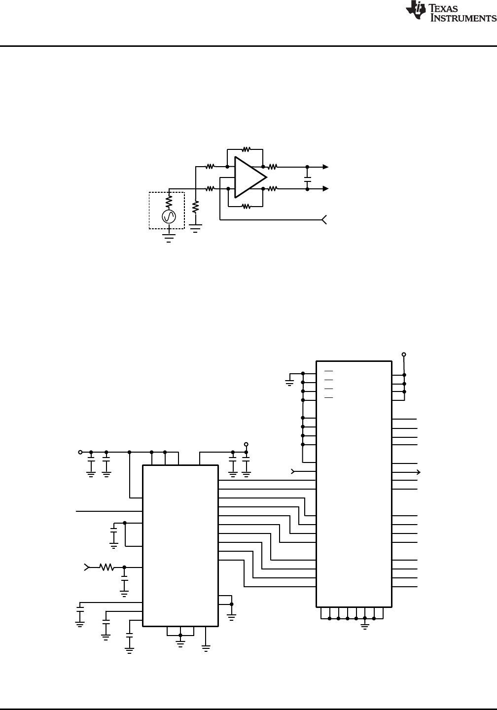
For very low frequency and DC input applications, a d.c. coupled amplifier or buffer may be needed, especially
when the input is single-ended and the advantages of a differential input signal is desired. Figure 41 shows the
input drive circuit that can be used to replace the transformer of Figure 40. The LMH6550 provides excellent
performance and is well-suited for this application. The common mode output voltage of the LMH6550 is the
same as its VCM input.
Figure 41. Using the LMH6550 for DC and wideband applications
Single Ended Applications
Performance of the ADC10040 with a single-ended input is not as good as its performance with a differential
input. However, if the lower performance is adequate, the circuit of Figure 42 shows an acceptable method of
driving the analog input.
Figure 42. A Simple Application Using a Single Ended Signal Source
20 Submit Documentation Feedback Copyright © 2003–2013, Texas Instruments Incorporated
Product Folder Links: ADC10040