
Datasheet


Table Of Contents
AIN
CLKIN
24 pF
0.1 PF
16:
16:
ADC10040
0.1 PF
0.1 PF
0.1 PF
V
REF
V
REFT
V
REFB
V
IN
+
V
IN
-
VCOM
CLK
0.1 PF
4.7 PF
V
DDA
IRS
V
DDA
V
DDA
V
DDA
V
SSA
V
SSA
V
SSA
V
SSIO
STBY
DF
V
DDA
74ACTQ16244
GND
GND
GND
GND
GND
GND
GND
GND
CLKIN
0.1 PF
4.7 PF
V
DDIO
V
DDIO
CLKOUT
21
12
1
5
4
13
8
6
7
14
11
3
28
15
16
17
18
19
20
23
24
25
26
27
22
10
9
2
43
44
46
47
41
40
37
38
36
35
33
30
29
27
26
48
25
24
1
32
21
15
10
28
34
39
45
4
31
42
7
23
22
19
17
16
14
13
12
11
9
8
6
5
3
2
18
20
D6
D7
D8
D9
D0
D1
D2
D3
D4
D5
3Y4
3Y3
3Y2
3Y1
2Y4
2Y3
2Y2
2Y1
1Y4
1Y3
1Y2
1Y1
4Y4
4Y3
4Y2
4Y1
V
CC
V
CC
V
CC
V
CC
4 OE
4A3
4A2
4A1
3A4
3A3
3A2
3A1
2A4
2A3
2A2
2A1
1A4
1A3
1A2
1A1
3 OE
1 OE
2 OE
D9
D8
D7
D6
D5
D4
D3
D2
D1
D0
ADC10040
www.ti.com
SNAS224M –JULY 2003–REVISED APRIL 2013
OUTPUT PINS
The ADC10040 has 10 TTL/CMOS compatible Data Output pins. The offset binary data is present at these
outputs while the DF and STBY pins are low. Be very careful when driving a high capacitance bus. The more
capacitance the output drivers must charge for each conversion, the more instantaneous digital current flows
through V
DDIO
and V
SSIO
. These large charging current spikes can cause on-chip noise and couple into the
analog circuitry, degrading dynamic performance. Adequate bypassing, limiting output capacitance and careful
attention to the ground plane will reduce this problem. Additionally, bus capacitance beyond the specified 10
pF/pin will cause t
OD
to increase, making it difficult to properly latch the ADC output data. The result could be an
apparent reduction in dynamic performance. To minimize noise due to output switching, minimize the load
currents at the digital outputs. This can be done by minimizing load capacitance and by connecting buffers
between the ADC outputs and any other circuitry, which will isolate the outputs from trace and other circuit
capacitances and limit the output currents, which could otherwise result in performance degradation. Only one
driven input should be connected to the ADC output pins.
While the t
OD
time provides information about output timing, a simple way to capture a valid output is to latch the
data on the rising edge of the conversion clock.
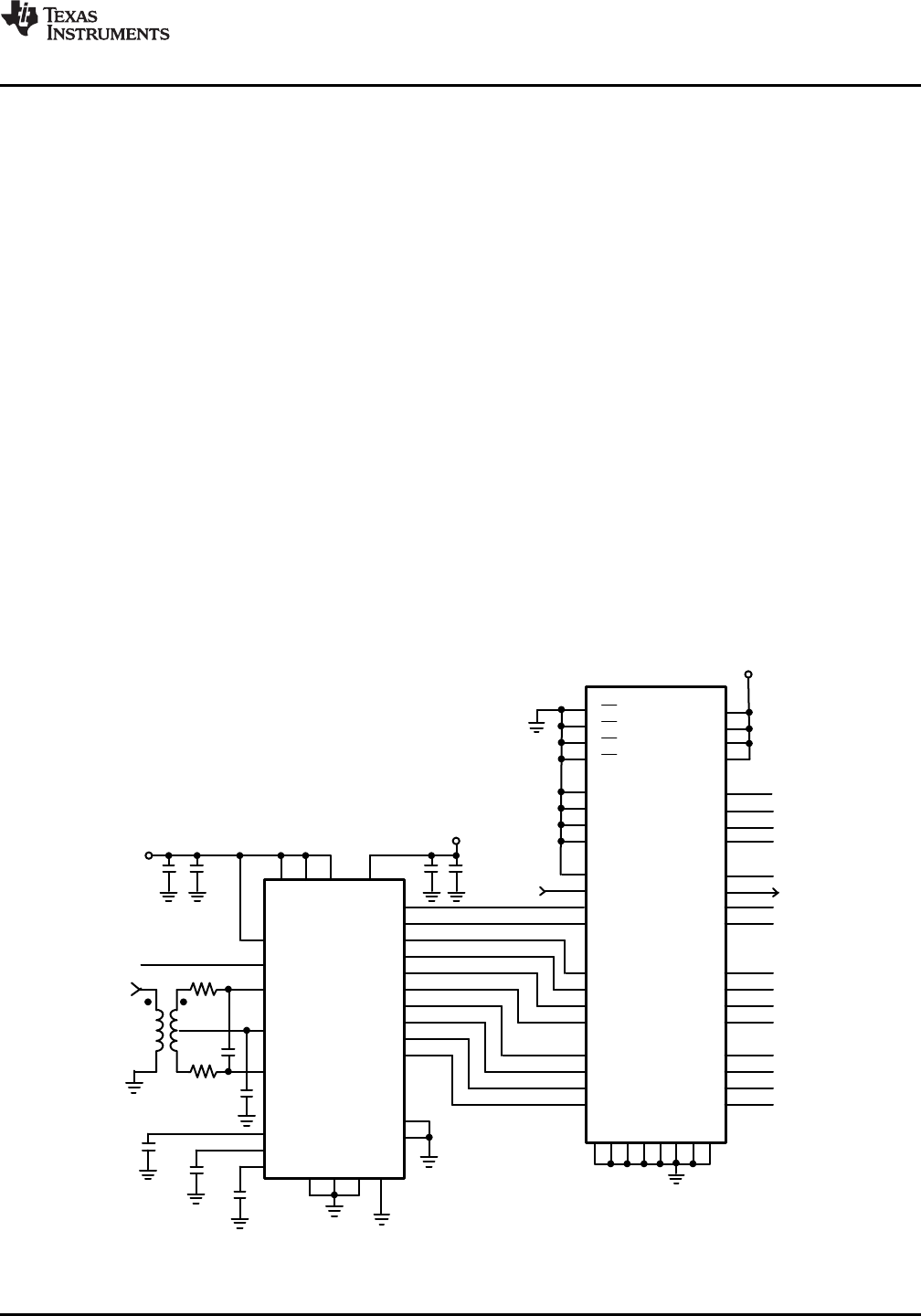
APPLICATION SCHEMATICS
The following figures show simple examples of using the ADC10040. The ADC10040 performs best with a
differential input signal.
Narrow Band A.C. Signals
Figure 40 shows a typical circuit for an AC coupled, differentially driven input. The 16Ω resistors and 24 pF
capacitor, together with the 4 pF input capacitance of the ADC10040, provides a −3dB input bandwidth of 177
MHz, while the 0.1µF capacitor at V
COM
stabilizes the common move voltage at the transformer center tap.
Figure 40. A Simple Application Using a Differential Signal Source
Copyright © 2003–2013, Texas Instruments Incorporated Submit Documentation Feedback 19
Product Folder Links: ADC10040