
Datasheet

ADC0820-N
SNAS529C –JUNE 1999–REVISED MARCH 2013
www.ti.com
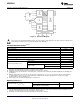
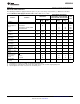
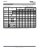
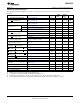
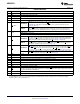
DC Electrical Characteristics
The following specifications apply for V
CC
= 5V, unless otherwise specified. Boldface limits apply from T
MIN
to T
MAX
; all
other limits T
A
= T
J
= 25°C.
ADC0820BCN, ADC0820CCN,
ADC0820CCJ ADC0820BCV, ADC0820BCWM,
Limit
ADC0820CCWM, ADC0820CIWM
Parameter Conditions
Units
Tested Design Tested Design
Typ
(1)
Typ
(1)
Limit
(2)
Limit
(3)
Limit
(2)
Limit
(3)
CS , WR , RD 2.0 2.0 2.0 V
V
IN(1)
, Logical “1”
V
CC
=5.25V
Input Voltage
Mode 3.5 3.5 3.5 V
CS , WR , RD 0.8 0.8 0.8 V
V
IN(0)
, Logical “0”
V
CC
=4.75V
Input Voltage
Mode 1.5 1.5 1.5 V
V
IN(1)
=5V; CS , RD 0.005 1 0.005 1 µA
I
IN(1)
, Logical “1”
V
IN(1)
=5V; WR 0.1 3 0.1 0.3 3 µA
Input Current
V
IN(1)
=5V; Mode 50 200 50 170 200 µA
I
IN(0)
, Logical “0” V
IN(0)
=0V; CS, RD, WR, Mode
−0.005 −1 −0.005 −1 µA
Input Current
V
CC
=4.75V, I
OUT
=−360 µA;
2.4 2.8 2.4 V
DB0–DB7, OFL , INT
V
OUT(1)
, Logical “1”
Output Voltage
V
CC
=4.75V, I
OUT
=−10 µA;
4.5 4.6 4.5 V
DB0–DB7, OFL , INT
V
OUT(0)
, Logical “0” V
CC
=4.75V, I
OUT
=1.6 mA;
0.4 0.34 0.4 V
Output Voltage DB0–DB7, OFL , INT , RDY
V
OUT
=5V; DB0–DB7, RDY 0.1 3 0.1 0.3 3 µA
I
OUT
, TRI-STATE
Output Current
V
OUT
=0V; DB0–DB7, RDY −0.1 −3 −0.1 −0.3 −3 µA
V
OUT
=0V; DB0–DB7, OFL −12 −6 −12 −7.2 −6 mA
I
SOURCE
, Output
Source Current
INT −9 −4.0 −9 −5.3 −4.0 mA
I
SINK
, Output Sink V
OUT
=5V; DB0–DB7, OFL ,
14 7 14 8.4 7 mA
Current INT , RDY
I
CC
, Supply Current CS =WR =RD =0 7.5 15 7.5 13 15 mA
(1) Typicals are at 25°C and represent most likely parametric norm.
(2) Tested limits are ensured to TI's AOQL (Average Outgoing Quality Level).
(3) Design limits are specified but not 100% tested. These limits are not used to calculate outgoing quality levels.
4 Submit Documentation Feedback Copyright © 1999–2013, Texas Instruments Incorporated
Product Folder Links: ADC0820-N