
Datasheet


ADC0820-N
www.ti.com
SNAS529C –JUNE 1999–REVISED MARCH 2013
Analog Considerations
REFERENCE AND INPUT
The two V
REF
inputs of the ADC0820-N are fully differential and define the zero to full-scale input range of the A
to D converter. This allows the designer to easily vary the span of the analog input since this range will be
equivalent to the voltage difference between V
IN
(+) and V
IN
(−). By reducing V
REF
(V
REF
= V
REF
(+) − V
REF
(−)) to
less than 5V, the sensitivity of the converter can be increased (i.e., if V
REF
= 2V then 1 LSB = 7.8 mV). The
input/reference arrangement also facilitates ratiometric operation and in many cases the chip power supply can
be used for transducer power as well as the V
REF
source.
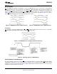
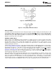
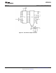
This reference flexibility lets the input span not only be varied but also offset from zero. The voltage at V
REF
(−)
sets the input level which produces a digital output of all zeroes. Though V
IN
is not itself differential, the reference
design affords nearly differential-input capability for most measurement applications. Figure 26 shows some of
the configurations that are possible.
INPUT CURRENT
Due to the unique conversion techniques employed by the ADC0820-N, the analog input behaves somewhat
differently than in conventional devices. The A/D's sampled-data comparators take varying amounts of input
current depending on which cycle the conversion is in.
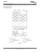
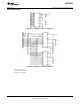
The equivalent input circuit of the ADC0820-N is shown in Figure 27. When a conversion starts (WR low, WR-RD
mode), all input switches close, connecting V
IN
to thirty-one 1 pF capacitors. Although the two 4-bit flash circuits
are not both in their compare cycle at the same time, V
IN
still sees all input capacitors at once. This is because
the MS flash converter is connected to the input during its compare interval and the LS flash is connected to the
input during its zeroing phase (see Architecture). In other words, the LS ADC uses V
IN
as its zero-phase input.
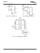
The input capacitors must charge to the input voltage through the on resistance of the analog switches (about 5
kΩ to 10 kΩ). In addition, about 12 pF of input stray capacitance must also be charged. For large source
resistances, the analog input can be modeled as an RC network as shown in Figure 28. As R
S
increases, it will
take longer for the input capacitance to charge.
In RD mode, the input switches are closed for approximately 800 ns at the start of the conversion. In WR-RD
mode, the time that the switches are closed to allow this charging is the time that WR is low. Since other factors
force this time to be at least 600 ns, input time constants of 100 ns can be accommodated without special
consideration. Typical total input capacitance values of 45 pF allow R
S
to be 1.5 kΩ without lengthening WR to
give V
IN
more time to settle.
External Reference 2.5V Full-Scale Power Supply as Reference Input Not Referred to GND
Figure 26. Analog Input Options
Copyright © 1999–2013, Texas Instruments Incorporated Submit Documentation Feedback 15
Product Folder Links: ADC0820-N